Epson S1C63558 User Manual
Page 147
S1C63558 TECHNICAL MANUAL
EPSON
137
CHAPTER 4: PERIPHERAL CIRCUITS AND OPERATION (FSK Demodulator)
Band-pass
filter
Carrier
detection circuit
Reference voltage
generation circuit
TIP
Amp
–
+
AV
SS
AV
DD
FSKIN
CDET
RDET
FOSC3
PWDN
RDIN
RING
FB
0.1
µ
F
RDRC
V
REF
V
DD
BPOUT
CDIN
FSK
demodulator
Clock
generator
Fig. 4.15.1.2 FSK core configuration
The external terminals of the FSK demodulator are as follows:
AV
DD
, AV
SS
Power terminals for the FSK block. Supply power respectively as AV
DD
= V
DD
, AV
SS
= V
SS
.
TIP
Inverted input terminal of the input amplifier
RING
Non-inverted input terminal of the input amplifier
FB
Feedback output terminal of the input amplifier
BPOUT
Output terminal of the band-pass filter
CDIN
Input terminal for carrier signal detection
RDIN
Input terminal for ring signal detection
RDRC
I/O terminal for connecting an RC network
V
RFF
Reference voltage (1/2V
DD
) output terminal
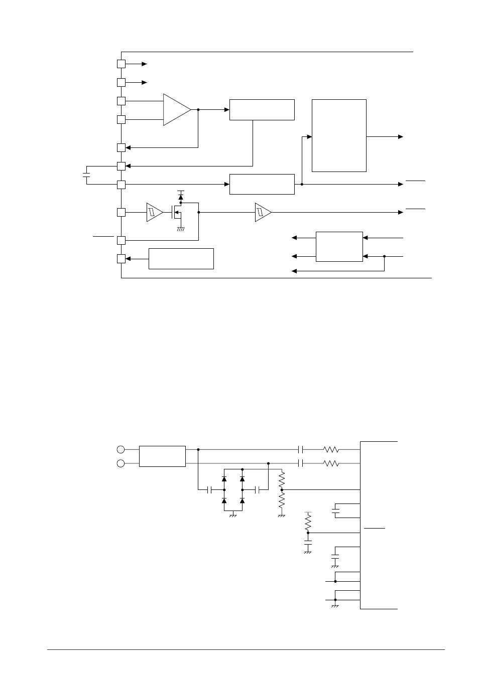
The basic external connection diagram is shown in Figure 4.15.1.3.
TIP
RING
FB
TIP
RING
RDIN
BPOUT
CDIN
RDRC
Protection
Network
0.2
µ
F
0.2
µ
F
470k
33k
10k
1000pF
1000pF
0.2
µ
F
0.1
µ
F
270k
10k
V
REF
AV
DD
V
DD
AV
SS
V
SS
0.1
µ
F
V
DD
Fig. 4.15.1.3 Basic external connection diagram (example for Bellcore)