4 i/o memory of input ports, And "0" when the voltage goes low (v – Epson S1C63558 User Manual
Page 40
30
EPSON
S1C63558 TECHNICAL MANUAL
CHAPTER 4: PERIPHERAL CIRCUITS AND OPERATION (Input Ports)
4.4.4 I/O memory of input ports
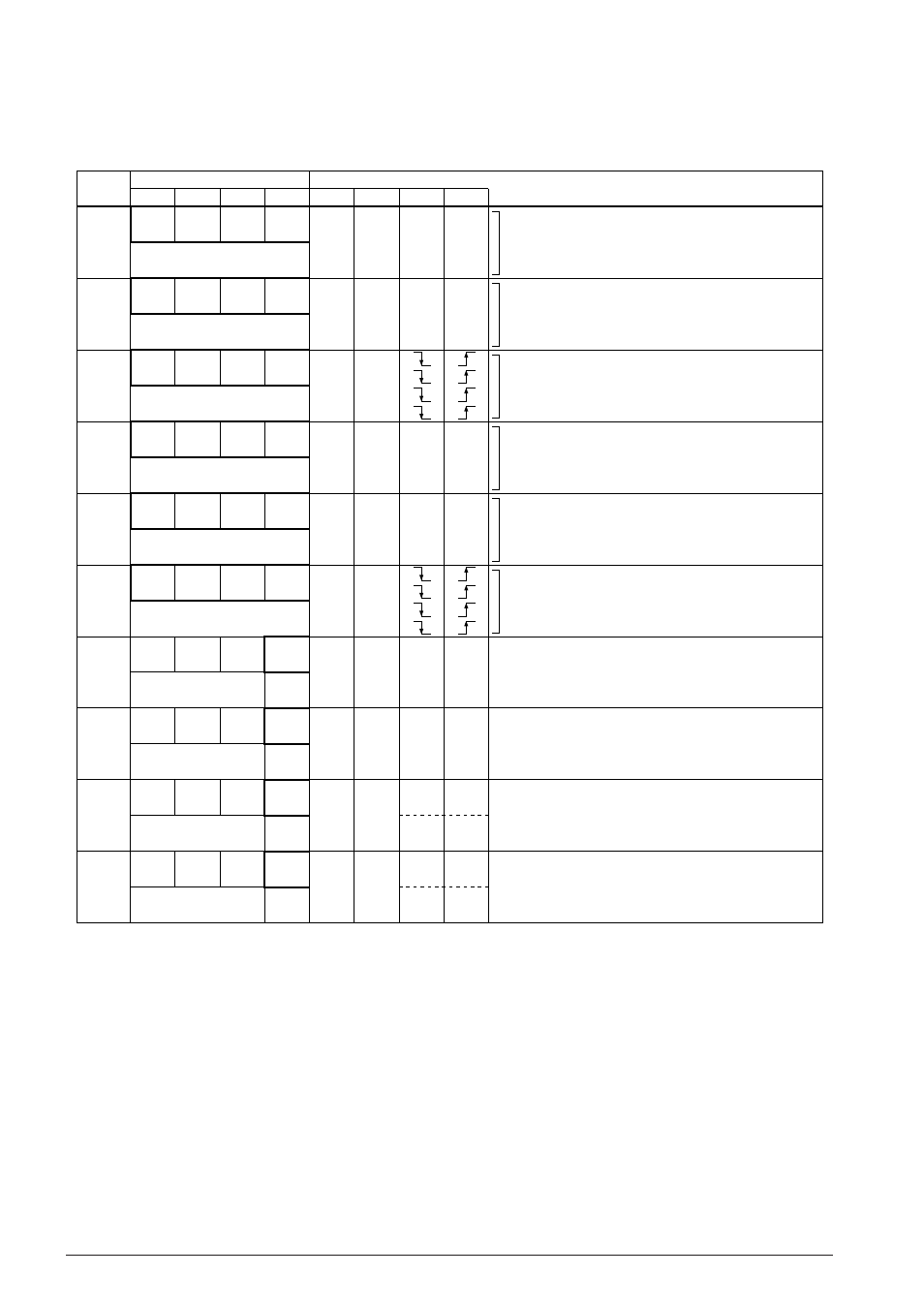
Table 4.4.4.1 shows the I/O addresses and the control bits for the input ports.
Table 4.4.4.1 Control bits of input ports
Address
Comment
D3
D2
Register
D1
D0
Name
Init
∗
1
1
0
FF20H
SIK03
SIK02
SIK01
SIK00
R/W
SIK03
SIK02
SIK01
SIK00
0
0
0
0
Enable
Enable
Enable
Enable
Disable
Disable
Disable
Disable
K00–K03 interrupt selection register
FF21H
K03
K02
K01
K00
R
K03
K02
K01
K00
–
∗
2
–
∗
2
–
∗
2
–
∗
2
High
High
High
High
Low
Low
Low
Low
K00–K03 input port data
FF22H
KCP03
KCP02
KCP01
KCP00
R/W
KCP03
KCP02
KCP01
KCP00
1
1
1
1
K00–K03 input comparison register
FF24H
SIK13
SIK12
SIK11
SIK10
R/W
SIK13
SIK12
SIK11
SIK10
0
0
0
0
Enable
Enable
Enable
Enable
Disable
Disable
Disable
Disable
K10–K13 interrupt selection register
FF25H
K13
K12
K11
K10
R
K13
K12
K11
K10
–
∗
2
–
∗
2
–
∗
2
–
∗
2
High
High
High
High
Low
Low
Low
Low
K10–K13 input port data
FF26H
KCP13
KCP12
KCP11
KCP10
R/W
KCP13
KCP12
KCP11
KCP10
1
1
1
1
K10–K13 input comparison register
FFE4H
0
0
0
EIK0
R
R/W
0
∗
3
0
∗
3
0
∗
3
EIK0
–
∗
2
–
∗
2
–
∗
2
0
Enable
Mask
Unused
Unused
Unused
Interrupt mask register (K00–K03)
FFE5H
0
0
0
EIK1
R
R/W
0
∗
3
0
∗
3
0
∗
3
EIK1
–
∗
2
–
∗
2
–
∗
2
0
Enable
Mask
Unused
Unused
Unused
Interrupt mask register (K10–K13)
FFF4H
0
0
0
IK0
R
R/W
0
∗
3
0
∗
3
0
∗
3
IK0
–
∗
2
–
∗
2
–
∗
2
0
(R)
Yes
(W)
Reset
(R)
No
(W)
Invalid
Unused
Unused
Unused
Interrupt factor flag (K00–K03)
FFF5H
0
0
0
IK1
R
R/W
0
∗
3
0
∗
3
0
∗
3
IK1
–
∗
2
–
∗
2
–
∗
2
0
(R)
Yes
(W)
Reset
(R)
No
(W)
Invalid
Unused
Unused
Unused
Interrupt factor flag (K10–K13)
*1 Initial value at initial reset
*2 Not set in the circuit
*3 Constantly "0" when being read
K00–K03: K0 port input port data (FF21H)
K10–K13: K1 port input port data (FF25H)
Input data of the input port terminals can be read with these registers.
When "1" is read: High level
When "0" is read: Low level
Writing: Invalid
The reading is "1" when the terminal voltage of the eight bits of the input ports (K00–K03, K10–K13) goes
high (V
DD
), and "0" when the voltage goes low (V
SS
).
These bits are dedicated for reading, so writing cannot be done.