Epson S1C63558 User Manual
Page 151
S1C63558 TECHNICAL MANUAL
EPSON
141
CHAPTER 4: PERIPHERAL CIRCUITS AND OPERATION (FSK Demodulator)
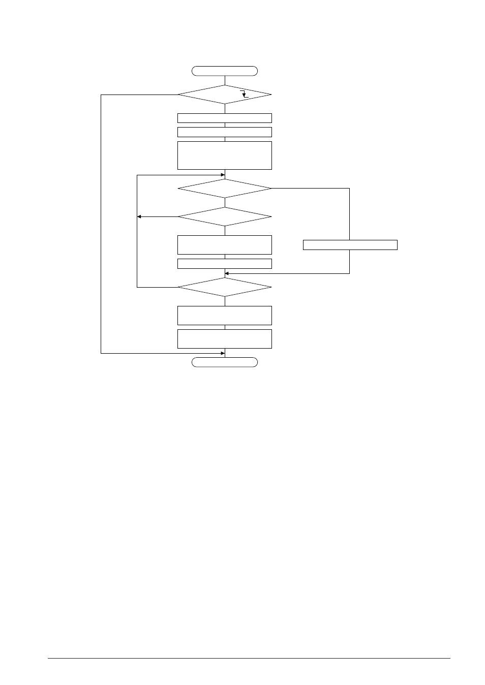
Data input procedure (example for Bellcore) is shown below.
FSK receiving
END
OSCC
←
1
RXTRGS
←
1
CLKCHG
←
1
FSKON
←
1
RXENS
←
1
RXENS
←
0
FSKON
←
0
CLKCHG
←
0
OSCC
←
0
5 msec wait
Received data reading
from TRXD0–TRXD7
1st RDET
Receiving error
Receiving complete
CDET
→
0
yes
yes
yes
yes
no
no
no
no
Error processing
Fig. 4.15.4.1 Data input flow (example for Bellcore)
1. Detect the falling edge (RDET = "0") of the first ring input. The ring detection interrupt can be used.
2. Turn the OSC3 oscillation circuit ON by writing "1" to OSCC.
3. After waiting 5 msec or more, switch the CPU operating clock from OSC1 to OSC3 by writing "1" to
CLKCHG.
4. Turn the FSK demodulator ON by writing "1" to FSKON.
5. Enable the serial interface (2) to receive data by writing "1" to RXENS.
6. Read data from TRXD0S–TRXD7S after waiting for the receiving interrupt of the serial interface (2).
After reading data, reset the overrun error check by writing "1" to RXTRGS. Repeat this step until the
carrier stops and a carrier detection interrupt is generated.
7. Disable data receiving by writing "0" to RXENS after the carrier stop detection interrupt is generated.
8. Turn the FSK demodulator OFF by writing "0" to FSKON.
9. Switch the CPU operating clock from OSC3 to OSC1 by writing "0" to CLKCHG.
10. Turn the OSC3 oscillation circuit OFF by writing "0" to OSCC.