3 high impedance control, 4 special output – Epson S1C63558 User Manual
Page 44
34
EPSON
S1C63558 TECHNICAL MANUAL
CHAPTER 4: PERIPHERAL CIRCUITS AND OPERATION (Output Ports)
4.5.3 High impedance control
The terminal output status of the output ports can be set to a high impedance status. This control is done
using the high impedance control register (RxxHIZ) corresponding to each output port (Rxx).
When "1" is written to the high impedance control register, the corresponding output port terminal goes
into high impedance status. When "0" is written, the port outputs a signal according to the data register.
4.5.4 Special output
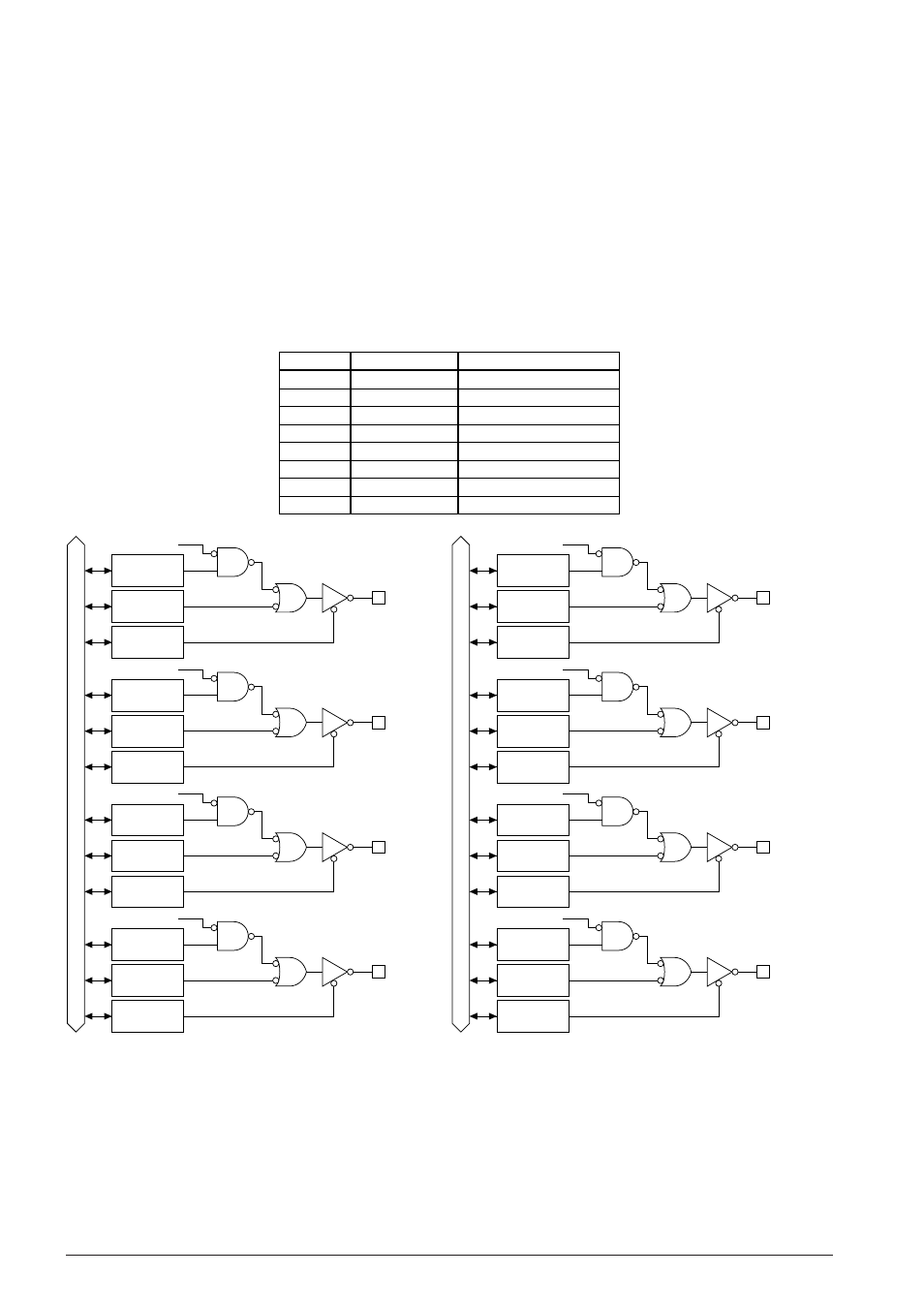
In addition to the regular DC output, special output can be selected for the output ports R00–R03 and
R10–R13 as shown in Table 4.5.4.1 with the software.
Figure 4.5.4.1 shows the configuration of the R00–R03 and R10–R13 output ports.
Table 4.5.4.1 Special output
Terminal
R13
R12
R11
R10
R03
R02
R01
R00
Special output
HFO
HDO
XRMUTE
XTMUTE
FOUT
TOUT
BZ
XBZ
Output control register
CHFO
CHDO
CRMO
CTMO
FOUTE
PTOUT
BZOUT
XBZOUT
Data bus
Register
FOUTE
Register
R03
Register
R03HIZ
FOUT
R03
(FOUT)
Register
PTOUT
Register
R02
Register
R02HIZ
TOUT
R02
(TOUT)
Register
BZOUT
Register
R01
Register
R01HIZ
BZ
R01
(BZ)
Register
XBZOUT
Register
R00
Register
R00HIZ
XBZ
R00
(XBZ)
Data bus
Register
CHFO
Register
R13
Register
R13HIZ
HFO
R13
(HFO)
Register
CHDO
Register
R12
Register
R12HIZ
HDO
R12
(HDO)
Register
CRMO
Register
R11
Register
R11HIZ
XRMUTE
R11
(XRMUTE)
Register
CTMO
Register
R10
Register
R10HIZ
XTMUTE
R10
(XTMUTE)
Fig. 4.5.4.1(a) Configuration of R00–R03 output ports Fig. 4.5.4.1(b) Configuration of R10–R13 output ports
At initial reset, the output port data register is set to "1" and the high impedance control register is set to
"0". Consequently, the output terminal goes high (V
DD
).
When using the output port (R00–R03, R10–R13) as the special output port, fix the data register (R00–R03,
R10–R13) at "1" and the high impedance control register (R00HIZ–R03HIZ, R10HIZ–R13HIZ) at "0" (data
output). The respective signal should be turned ON and OFF using the special output control register.