4 register descriptions, 1 the reset register – Sundance SMT381 2004 User Manual
Page 45
+ A pre-read is generated on the first read. A second read is required to read the real
data.
Table 3. Register Memory Map (DAC registers not yet fixed in firmware)
For registers larger than 16 bits with an LSB and MSB part always write the LSB part
first and then the MSB.
5.4 Register Descriptions
5.4.1 The Reset Register
As with normal register reading (command 0x2) and writing (command 0x1), there is
a command defined for reset. This is command 0xF. The reset command will write to
a reset register. Writing 0x0001 to it will keep the FPGA in reset, and writing 0x0000
to it will take the FPGA out of reset. This register is at address 0x000.
31 .. 28
27 .. 24
23 .. 20
19 .. 16
15 .. 12
11 .. 8
7 .. 4
3 .. 0
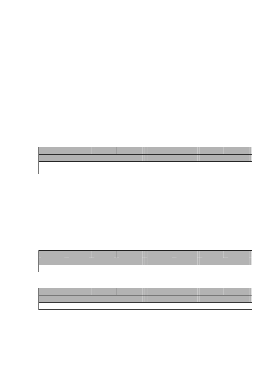
Command
Address
Data MSB
Data LSB
0xF
0xF
0x000
0x000
0x00
0x00
0x00 – Not in Reset
0x01 – FPGA in Reset
Figure 25. Reset Register (Write Only).
5.4.2 Firmware Version Register (Read Add 0x000)
A read from address 0x000 will display the firmware version register. The value of
this register is hard coded during VHDL compiles and must be stepped for each new
version of the firmware. Even though 32 bits are read over the ComPort, the firmware
version register is a 16 bit register (16 least significant bits of the returned value).
Read Request Format:
31 .. 28
27 .. 24
23 .. 20
19 .. 16
15 .. 12
11 .. 8
7 .. 4
3 .. 0
Command
Address
Data MSB
Data LSB
0x2
0x000
xx
xx
Read Response Format:
31 .. 28
27 .. 24
23 .. 20
19 .. 16
15 .. 12
11 .. 8
7 .. 4
3 .. 0
Command
Address
Data MSB
Data LSB
0x2
0x000
Firmware Version
Firmware Version
Figure 26. Firmware Version Register (Read Only).