5 control register settings, 1 control packet structure, The defined commands are – Sundance SMT381 2004 User Manual
Page 41
5 Control Register Settings
The Control Registers in the SMT381 example firmware control the complete
functionality of the SMT381-VP. These Control Registers are setup via ComPort 3.
The settings of the DAC, the trigger settings, the clock settings, the configuration of
the SHB and RSL interfaces and the internal FPGA data path settings can be
configured via the Control Registers.
5.1 Control Packet Structure
The data passed on to the SMT381 over the ComPorts must conform to a certain
packet structure (for compatibility with example firmware). Only valid packets will be
accepted and only after acceptance of a packet will the appropriate settings be
implemented. Each packet will start with a certain command indicating a write (0x1)
or a read (0x2). The address to write the data payload into (or where to read from)
will follow next. After the address the data will follow.
A 32-bit packet is received on ComPort3 and decoded. A write command will write
data into a register. A read command will request data from the FPGA. Once the data
is collected it will be transmitted over ComPort3. When issuing a read command the
return value must first be received before issuing the next read command.
All maximum size of registers that can be written to or read is 16 Bits. When
performing a read bits 31 downto 16 will reflect the command and address. The lower
16 bits will contain the actual data.
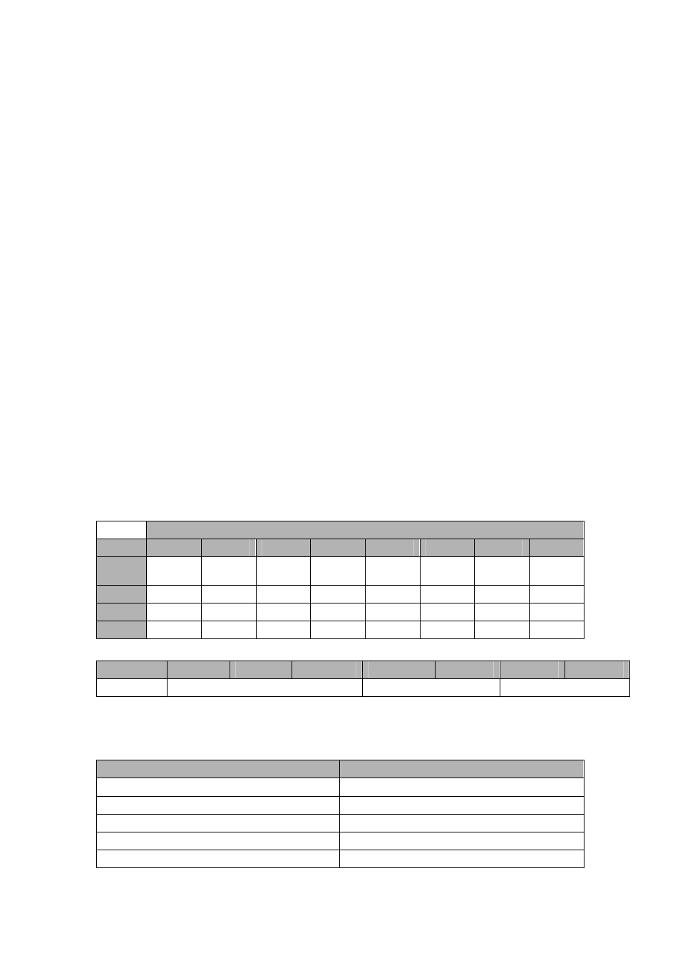
This structure is illustrated in the following figure:
Byte Content
Byte
Bit 7
Bit 6
Bit 5
Bit 4
Bit 3
Bit 2
Bit 1
Bit 0
3
Cmnd 3
Cmnd 2
Cmnd 1
Cmnd 0
Address
11
Address
10
Address 9
Address 8
2
Address 7
Address 6
Address 5
Address 4
Address 3
Address 2
Address 1
Address 0
1
Data 15
Data 14
Data 13
Data 12
Data 11
Data 10
Data 9
Data 8
0
Data 7
Data 6
Data 5
Data 4
Data 3
Data 2
Data 1
Data 0
Or
31 .. 28
27 .. 24
23 .. 20
19 .. 16
15 .. 12
11 .. 8
7 .. 4
3 .. 0
Command
Address
Data MSB
Data LSB
Figure 22. Setup Packet Structure.
The defined commands are:
Command Value
Command Description
0x0
Reserved
0x1
FGPA Write
0x2
FPGA Read
0x3
Reserved
0x4
Reserved