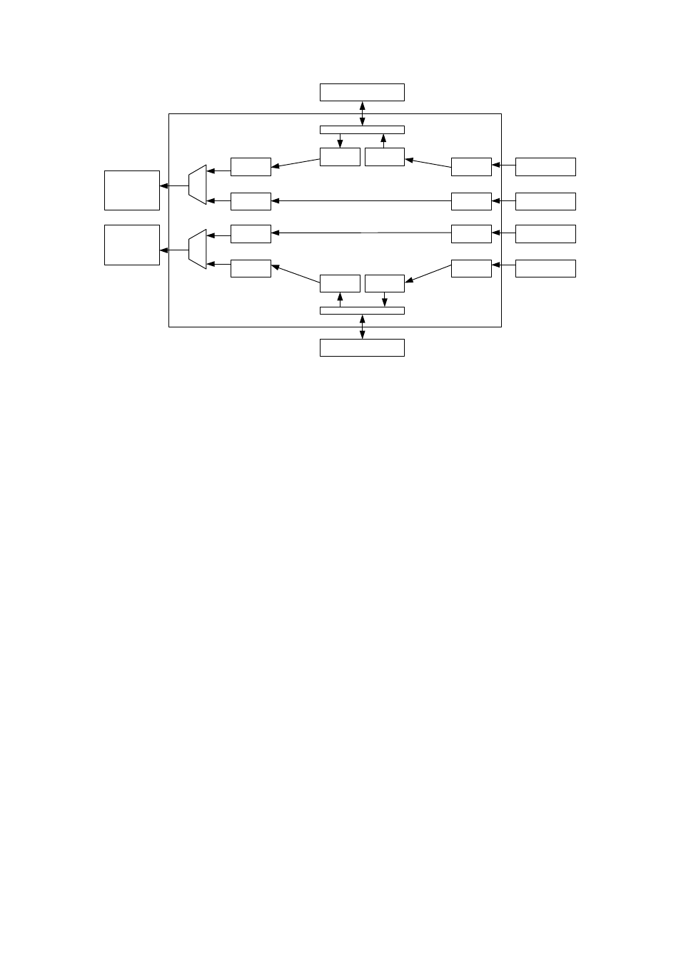
1 description of internal fpga blocks, Figure 2. internal data path of the smt338-vp – Sundance SMT381 2004 User Manual
Page 15
DAC
Channel A
DDR SDRAM
RSL for Channel A
SHB for Channel A
SI
Pre-process
Data
Retrieve from
Memory
SHB
Interface
Pre-process
Data
Store in
Memory
Memory Interface
Pre-process
Data
Pre-process
Data
Retrieve from
Memory
Store in
Memory
Memory Interface
DDR SDRAM
SI
SHB
Interface
SHB for Channel B
RSL for Channel B
DAC
Channel B
Mux
Mux
Figure 2. Internal Data path of the SMT338-VP.
The digital data stream is received from two interfaces. The first data stream is a
direct RSL interface for real-time type applications (RSL is not yet implemented).
While the second stream comes from the DDR SDRAM memory for non-real-time
type module transmits (the memory is initialized over the SHB interface).
Each data stream is then conditioned and sent to the SMT381 via the daughter card
connector. A multiplexer selects between the two data streams.
2.5.1 Description of internal FPGA blocks
Pre-processing Data
The user can implement his own type of processing on the data stream if required.
SI
The Serial Interface block takes the high-speed serial input data stream and converts
it into a parallel data stream (Not yet implemented).
Mux
The multiplexer connected to the RSL and SHB/memory interfaces selects between
these two data streams to send to the SMT381.
Store in Memory
The store in memory block takes the incoming data stream from the SHB and stores
the data into DDR SDRAM. This block will only transfer data from the memory to the
SMT381 when a valid trigger command is received. The amount of data that must be
stored is configurable.