Sundance SMT381 2004 User Manual
Page 43
Sending 0x2801xxxx over ComPort3 from the Host to the SMT381-VP will request a
Read, from Address 0x801. Once this command is received by the SMT381-VP, the
requested data will automatically be transmitted back over ComPort 3, following the
same packet structure.
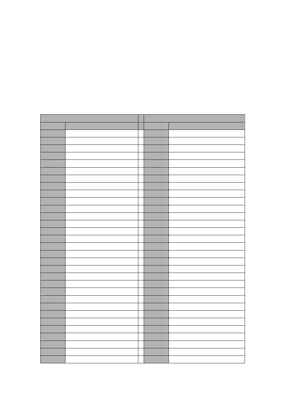
5.3 Memory Map
The write packets must contain the address where the data must be written to and
the read packets must contain the address where the required data must be read.
The following figure shows the memory map for the writable and readable Control
Registers on the SMT381-VP:
Write Side
Read Side
Address
Register
Address
Register
0x000
Reserved
0x000
FirmwareVersion
0x001
ComInScratchReg0
0x001
ComOutScratchReg0
0x002
ComInScratchReg1
0x002
ComOutScratchReg1
0x003
ShbACntrlReg
0x003
ShbAStatusReg
0x004
ShbBCntrlReg
0x004
ShbBStatusReg
0x005
ShbAComTestWordInLsb
0x005
ShbAComTestWordOutLsb
0x006
ShbAComTestWordInMsb *
0x006
ShbAComTestWordOutMsb
0x007
ShbBComTestWordInLsb
0x007
ShbBComTestWordOutLsb
0x008
ShbBComTestWordInMsb *
0x008
ShbBComTestWordOutMsb
0x009
Reserved
0x009
Reserved
0x00A
Reserved
0x00A
Reserved
0x00B
Reserved
0x00B
Reserved
0x00C
Reserved
0x00C
Reserved
0x00D
Reserved
0x00D
Reserved
0x00E
DdrACPCntrlReg
0x00E
DdrACPStatusReg
0x00F
DdrBCPCntrlReg
0x00F
DdrBCPStatusReg
0x010
DdrACPCommand0In
0x010
Reserved
0x011
DdrACPCommand1In
0x011
Reserved
0x012
DdrACPCommand2In
0x012
Reserved
0x013
DdrACPCommand3In *
0x013
Reserved
0x014
DdrACPData0In
0x014
DdrACPData0Out
0x015
DdrACPData1In
0x015
DdrACPData1Out
0x016
DdrACPData2In
0x016
DdrACPData2Out
0x017
DdrACPData3In *
0x017
DdrACPData3Out +
0x018
DdrBCPCommand0In
0x018
Reserved
0x019
DdrBCPCommand1In
0x019
Reserved
0x01A
DdrBCPCommand2In
0x01A
Reserved
0x01B
DdrBCPCommand3In *
0x01B
Reserved
0x01C
DdrBCPData0In
0x01C
DdrBCPData0Out
0x01D
DdrBCPData1In
0x01D
DdrBCPData1Out
0x01E
DdrBCPData2In
0x01E
DdrBCPData2Out