8 power supply and reset structure – Sundance SMT381 2004 User Manual
Page 19
•
Transmit a pre-determined amount of samples when a trigger is received, and
carry on cycling through them.
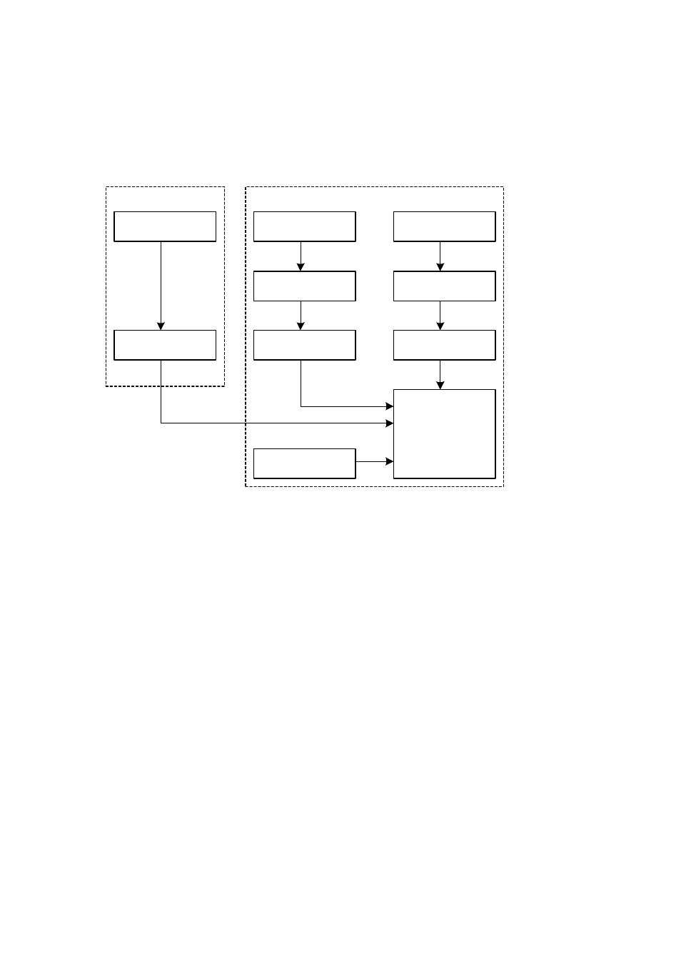
The following diagram is a graphical representation of the trigger structure and
sources on the SMT381 and SMT338-VP:
FPGA
External Trigger
LVPECL
Buffer
External Trigger Input
(MMBX)
ComPort Rx Cmd
State Machine
ComPort Interface
Trigger Generation
RSL Rx Cmd State
Machine
RSL CDR Interface
Trigger Generation
Trigger
Distribution
Trigger Setup
Register
SMT381
SMT338-VP
Figure 4. Trigger structure of the SMT381 and SMT338-VP.
2.8 Power Supply and Reset Structure
The SMT381 uses the following voltages: 12V, -12V, 5V, -5.2V, 3.3V and 1.8V. Only
two voltages must be generated on the SMT381 as the rest are supplied by the
carrier. The voltages that must be generated are -5.2V and 1.8V. -5.2V is used for
the comparator and op amp in the clock circuitry while 1.8V is used for the serial
control interface on the DAC.
All the other voltages are supplied by the carrier and thus present on the SMT338-
VP. The required voltages are then supplied to the SMT381 by a daughter card
power connector present on the SMT338-VP and SMT381. The SMT381 plugs into
this power connector and thus has power for all its modules.
Pin X_RESET is the only reset option on the SMT381. This pin resides on the DAC.
On the falling edge of X_RESET the DAC is reset and all registers are set to their
default values. After a reset most parts of the device are powered down.
The following figure shows the power structure of the SMT338-VP and SMT381: