2 functional description, 1 module overview, Figure 1. functional block diagram of smt381 – Sundance SMT381 2004 User Manual
Page 12
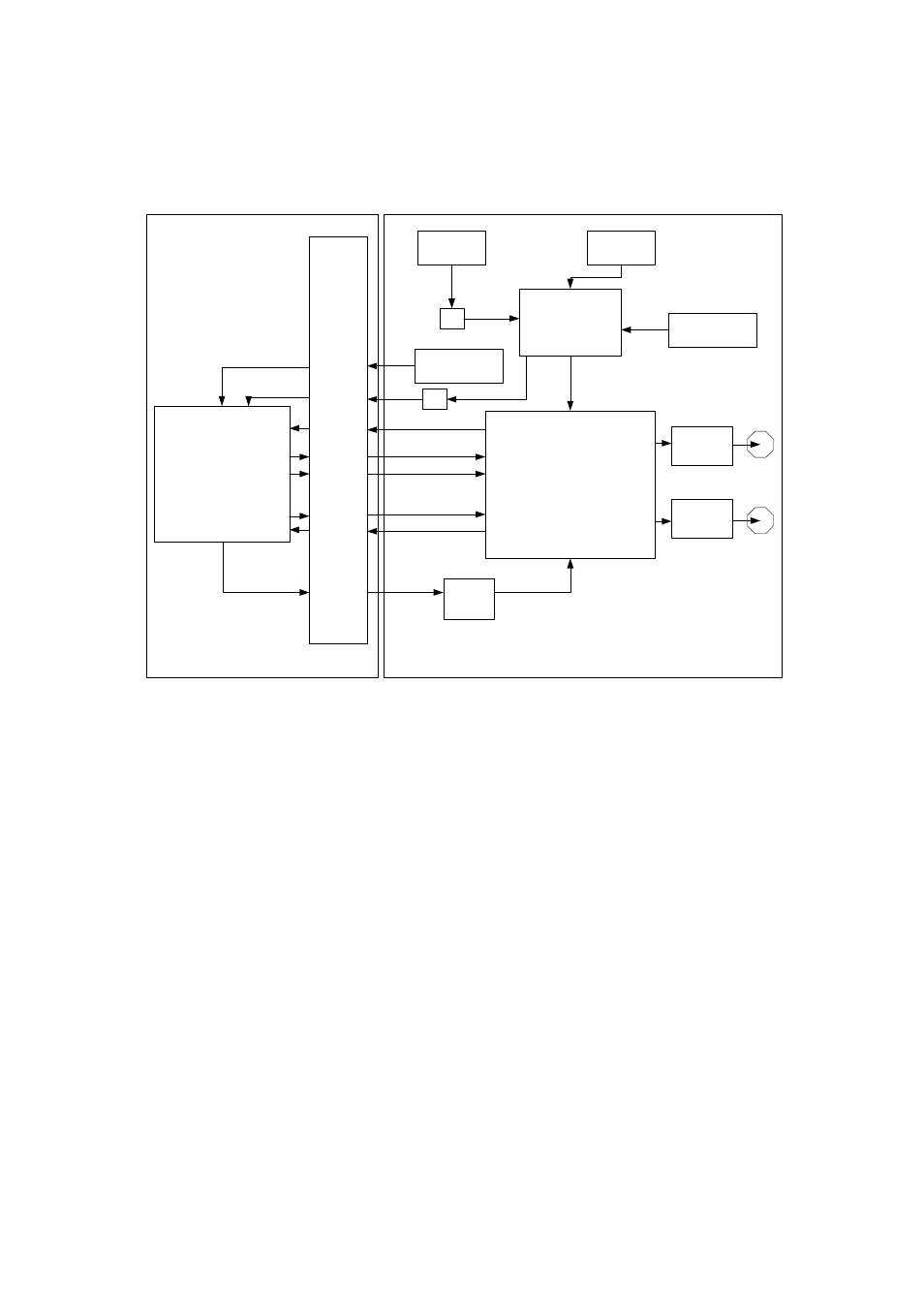
2 Functional Description
2.1 Module Overview
Digital to Analog
Convertor
(MB86064)
LVPECL
Clock Generation
and
Distribution
600MHz -
1200MHz
VCO
25MHz -
400MHz
Clock Synth
div
2
SMT338
FPGA
Ext
Trigger
Ch A and Ch B
Daughter
Card
Connector
Signal
Conditioning
Ch
A
Ch
B
Signal
Conditioning
1V8
Convertor
circuit
External Clock
div
8
Input Clock
(1d)
Input Clock (1d)
Data Sync Clock (1d)
Data Channel A (14d)
Data Channel B (14d)
Loop Clock (1d)
Loop Clock (1d)
Ext
Trigger
(1d)
Output
CHA
Output
CHB
Control (4)
SMT381
SMT338-VP
The numbers in brackes denote the
amount of FPGA IO pins requires.
'd' is used for differential pairs. 1d
Will thus requre 2 IOs
Notes:
Figure 1. Functional Block diagram of SMT381.
The SMT338-VP sends the digital data to the module via the daughter card
connector. Data is clocked out of the FPGA on both edges of the DAC clock (DDR).
The user can provide this clock by means of the VCO, Clock synthesizer or custom
external clock. The external clock can be provided as an LVPECL clock or as an RF
clock (two separate inputs).
All digital functions on the module are controlled by the SMT338-VP. There are two
14-bit LVDS ports on the DAC which converts the data on a DDR clock. The sampled
data can either be supplied to the DAC cores externally via the LVDS data bus or
internally from the Waveform Memory Module. The data may be routed to the DAC
cores through a number of paths. The most direct path routes data straight from the
LVDS input buffers to the DAC core input latches.
There are two DAC cores present in the MB86064. Thus two channels are available
for outputs. The outputs of the DAC are differential currents, which are converted to a
voltage by the analogue output stage. Details on the set up will be discussed later.
The design of the SMT381 is split over two PCBs. The main PCB (main module –
SMT338-VP) contains the FPGA and the digital connector interfaces (TIM, SHB and