2 block diagram, Figure 4-1, Block diagram of mvme8100 – Artesyn MVME8100/MVME8110 Installation and Use (September 2014) User Manual
Page 72: Functional description
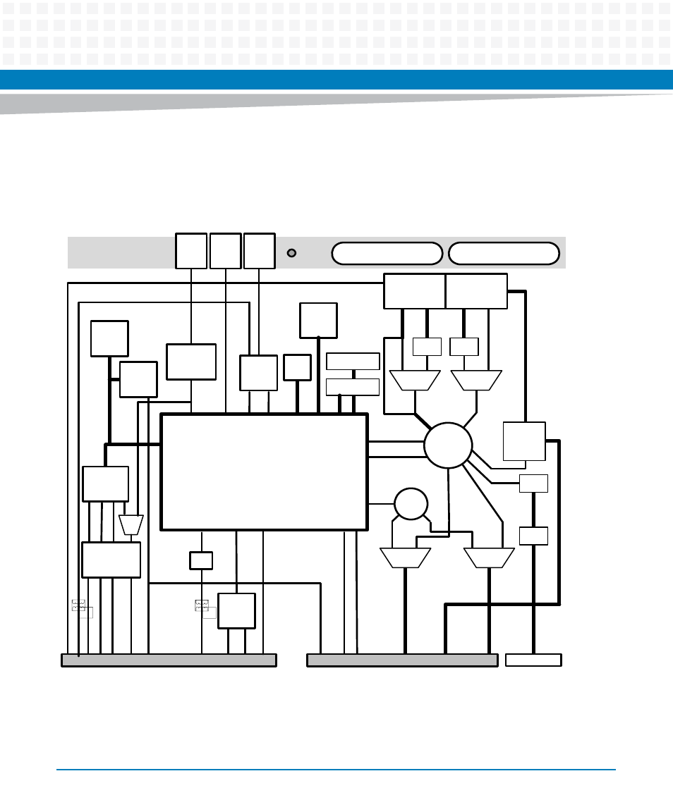
Functional Description
MVME8100 / MVME8110 Installation and Use (6806800P25G)
72
4.2
Block Diagram
illustrates the MVME8100 architecture.
Figure 4-1
Block Diagram of MVME8100
USB
16MB
Flash
8GB
eMMC
MUX/
DEMUX
1
PCIe to
PCI-X
PMC/ XMC/2.5 "
HDD/SSD
Site 2
64- bit
133MHz
PCI-X
PCIe x4
PCIe x8
PCIe x4
PCIe x4
MUX/
DEMUX
0
PCIe to
PCI-X
PCIe x4
PCIe x4
PCIe x8
PCIe x4
PMC/ XMC
Site 1
PCIe x4
PCIe x4
PCIe x4 ( NTB)
PCIe x4
( NTB)
sRIO x4
sRIO x4
sRIO x4
MUX/
DEMUX
3
MUX/
DEMUX
2
PCIe Switch
sRIO
Switch
PCIe x1
PCIe to
PCI-X
IDT
TSI148
64- bit
133MHz
PCI-X
VM
E
B
u
s
SATA
SA
TA
DDR3+ECC
DDR3+ECC
SATA
CTRL
SDHC
SG
M
II
SG
M
II
SG
M
II
PHY1
1
0
00
B
A
SE-
T
RG
M
II
RG
M
II
Dual
PHY
1
000
BASE
-T
10
00
B
A
SE
-T
10
00B
A
S
E
-T
SPI
RJ45
MAG
JACK
USB
US
B
USB
Hub
Quad
UART
RS
-XXX
RS
-XXX
RS
-XXX
RS
-XXX
Multi- Protocol
Transceiver
4 Multi- Protocol
Transceivers
USB
PORT
Freescale
QorIQ P5020
RS
-X
XX
Micro
DB9
PMC/ XMC I/ O 1
PMC/ XMC I/ O 2
512kB
MRAM
Local
Bus
UAR
T
UAR
T
UA
RT
UA
R
T
2
P 4 I/O
P 2 RTM
x2
G
P
IO
s
P0
CPLD
P1 , P 2 BP
Front Panel
NOTE:
Front panel connectors are not
assembled on conduction
- cooled
variant.
PCIe x2
M
U
X
RESET
PM
C
1
P
4
I/
O
I2C
x2
GP
IO
s
X4
S
E
R
IA
L
X4
SER
IA
L