Address clock enable support, Address clock enable during read cycle waveform, Address clock enable support -5 – Altera MAX 10 Embedded Memory User Manual
Page 9
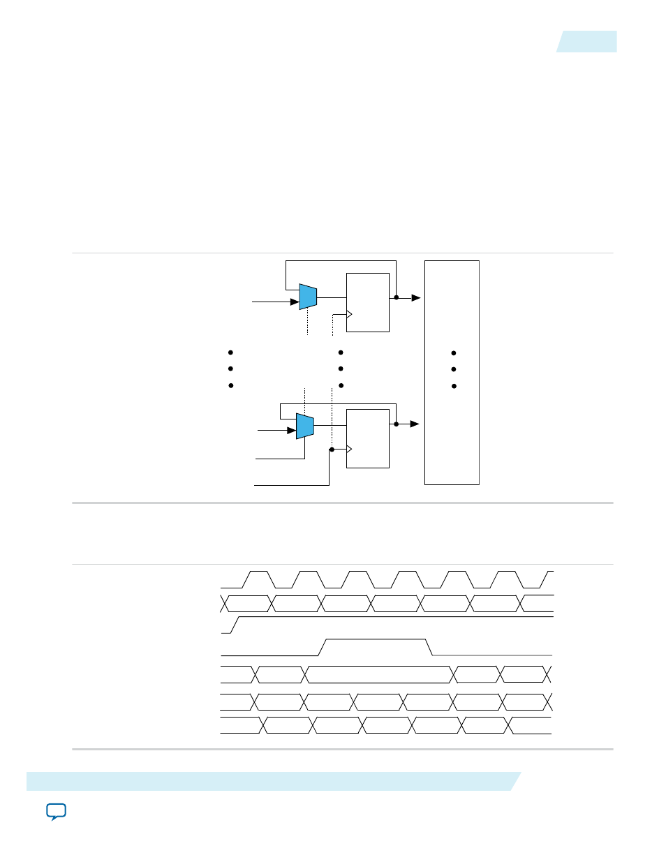
Address Clock Enable Support
• The address clock enable feature holds the previous address value for as long as the address clock
enable signal (
addressstall
) is enabled (
addressstall = 1
).
• When you configure M9K memory blocks in dual-port mode, each port has its own independent
address clock enable.
• Use the address clock enable feature to improve the effectiveness of cache memory applications during
a cache-miss.
• The default value for the
addressstall
signal is low.
• The address register output feeds back to its input using a multiplexer. The
addressstall
signal
selects the multiplexer output.
Figure 2-3: Address Clock Enable Block Diagram
address[0]
address[N]
addressstall
clock
address[0]
register
address[N]
register
address[N]
address[0]
Address Clock Enable During Read Cycle Waveform
Figure 2-4: Address Clock Enable Waveform During Read Cycle
inclock
rden
rdaddress
q (synch)
a0
a1
a2
a3
a4
a5
a6
q (asynch)
an
a0
a4
a5
latched address
(inside memory)
dout0
dout1
dout1 dout4
dout1
dout4 dout5
addressstall
a1
doutn-1
dout1
doutn
doutn
dout1
dout0
dout1
UG-M10MEMORY
2015.05.04
Address Clock Enable Support
2-5
MAX 10 Embedded Memory Architecture and Features
Altera Corporation