Address clock enable during write cycle waveform, Asynchronous clear, Asynchronous clear -6 – Altera MAX 10 Embedded Memory User Manual
Page 10
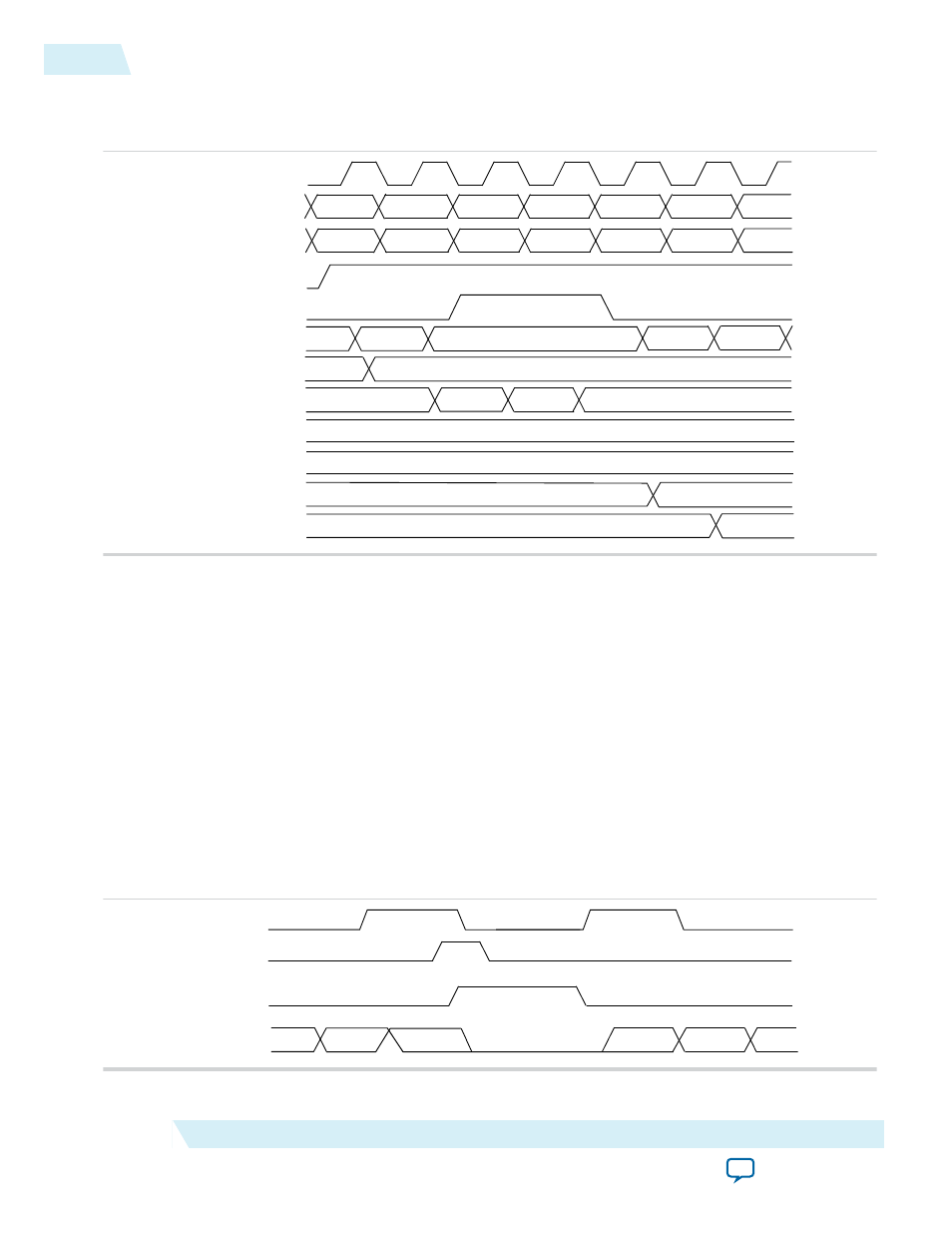
Address Clock Enable During Write Cycle Waveform
Figure 2-5: Address Clock Enable Waveform During Write Cycle
inclock
wren
wraddress
a0
a1
a2
a3
a4
a5
a6
an
a0
a4
a5
latched address
(inside memory)
addressstall
a1
data
00
01
02
03
04
05
06
contents at a0
contents at a1
contents at a2
contents at a3
contents at a4
contents at a5
XX
04
XX
00
03
01
XX
02
XX
XX
XX
05
Asynchronous Clear
You can selectively enable asynchronous clear per logical memory using the RAM: 1-PORT and RAM: 2-
PORT IP cores.
The M9k block supports asynchronous clear for:
• Read address registers: Asserting asynchronous clear to the read address register during a read
operation might corrupt the memory content.
• Output registers: When applied to output registers, the asynchronous clear signal clears the output
registers and the effects are immediately seen. If your RAM does not use output registers, you can still
clear the RAM outputs using the output latch asynchronous clear feature.
• Output latches
Note: Input registers other than read address registers are not supported.
Figure 2-6: Output Latch Asynchronous Clear Waveform
aclr
aclr at latch
clk
q
a1
a0
a1
a2
2-6
Address Clock Enable During Write Cycle Waveform
UG-M10MEMORY
2015.05.04
Altera Corporation
MAX 10 Embedded Memory Architecture and Features