Data byte output, Ram blocks operations, Packed mode support – Altera MAX 10 Embedded Memory User Manual
Page 8: Packed mode support -4
Data Byte Output
If you...
...Then
Deassert a byte-enable bit during a write cycle
The old data in the memory appears in the
corresponding data-byte output.
Assert a byte-enable bit during a write cycle
The corresponding data-byte output depends on the
Quartus
®
II software setting. The setting can be
either the newly written data or the old data at that
location.
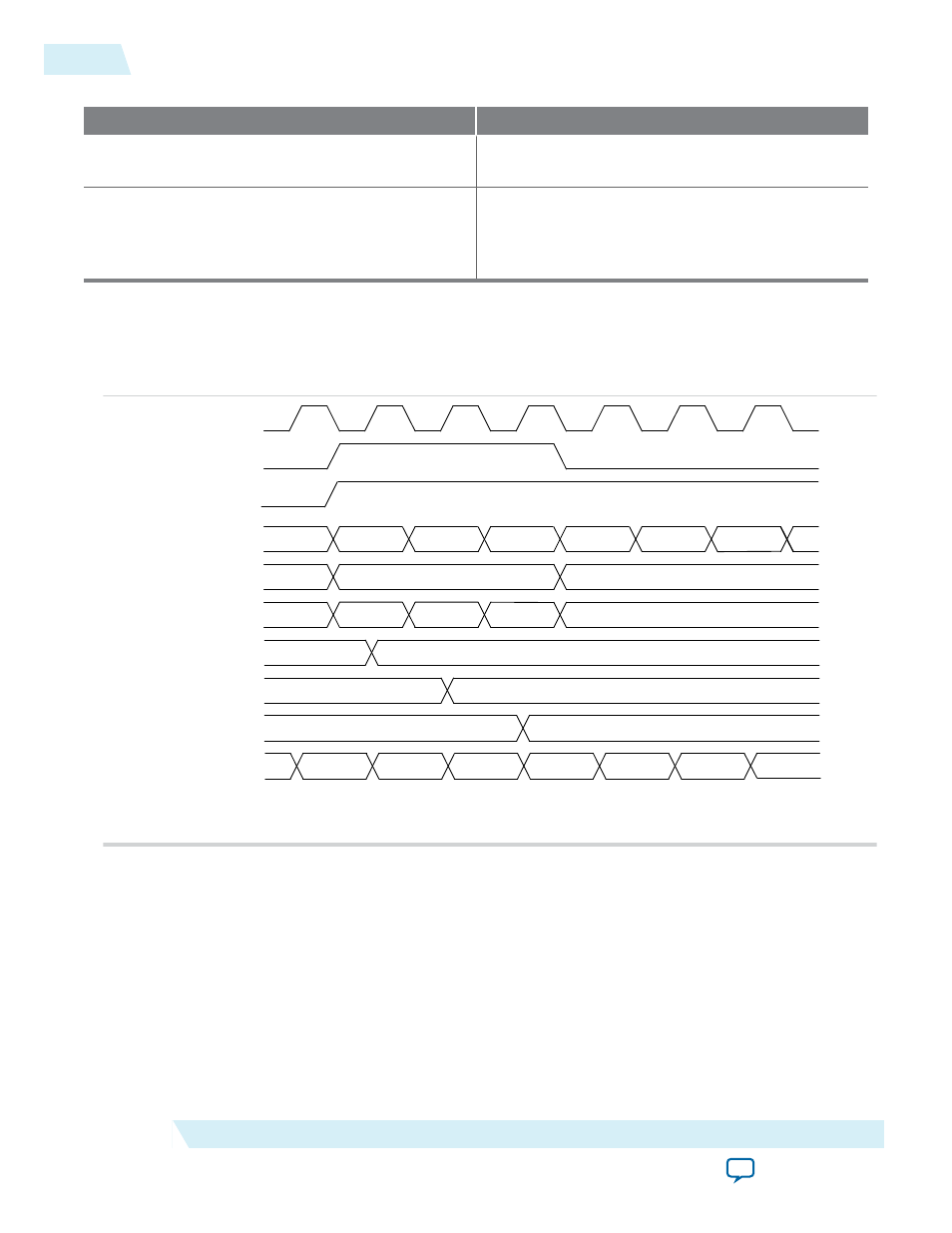
RAM Blocks Operations
This figure shows how the
wren
and
byteena
signals control the RAM operations.
Figure 2-2: Byte Enable Functional Waveform
inclock
wren
address
data
q (asynch)
an
XXXX
a0
a1
a2
a0
a1
a2
doutn
ABFF
FFCD
ABCD
ABFF
FFCD
ABCD
byteena
XX
10
01
11
XXXX
XX
ABCD
ABCD
FFFF
FFFF
FFFF
ABFF
FFCD
contents at a0
contents at a1
contents at a2
rden
For this functional waveform, New Data Mode is selected.
Packed Mode Support
You can implement two single-port memory blocks in a single block under the following conditions:
• Each of the two independent block sizes is less than or equal to half of the M9K block size. The
maximum data width for each independent block is 18 bits wide.
• Each of the single-port memory blocks is configured in single-clock mode.
Related Information
MAX 10 Embedded Memory Clock Modes
on page 2-9
2-4
Data Byte Output
UG-M10MEMORY
2015.05.04
Altera Corporation
MAX 10 Embedded Memory Architecture and Features