Iguration, Table 4.d, Table – Rockwell Automation 20-COMM-Q ControlNet Adapter User Manual
Page 65: Table 4.f
Configuring the I/O
4-29
20-COMM-C/Q ControlNet Adapter User Manual
Publication 20COMM-UM003F-EN-P
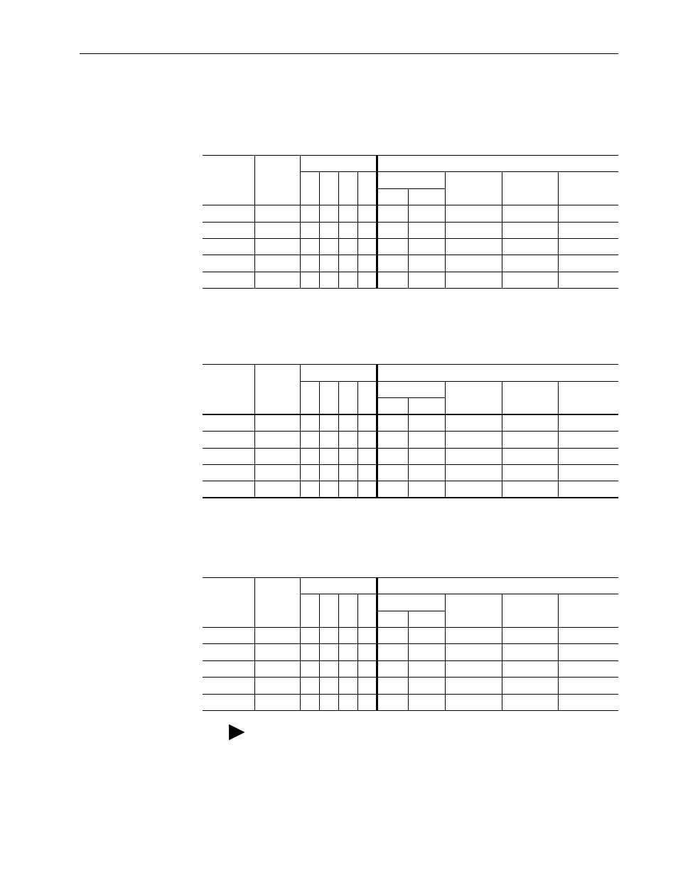
Table 4.D Drives with 16-bit Reference/Feedback and 16-bit Datalinks
These products include the following:
Table 4.E Drives with 16-bit Reference/Feedback and 32-bit Datalinks
These products include the following:
Table 4.F Drives with 32-bit Reference/Feedback and 32-bit Datalinks
These products include the following:
11. Click OK.
• PowerFlex 70 drives with standard or enhanced control
• SMC Flex smart motor controllers
• PowerFlex 700 drives with standard control
• SMC-50 smart motor controllers
• PowerFlex 700H drives
Logic
Command/
Status
Ref/Fdbk
(16-bit)
Datalinks (16-bit)
User Configured Settings
A
B
C
D
Size in Words
Par. 13 -
[DPI I/O Cfg]
Par. 25 -
[M-S Input]
Par. 26 -
[M-S Output]
Input
Output
✔
✔
2
2
…0 0001
…0 0001
…0 0001
✔
✔
✔
4
4
…0 0011
…0 0011
…0 0011
✔
✔
✔
✔
6
6
…0 0111
…0 0111
…0 0111
✔
✔
✔
✔
✔
8
8
…0 1111
…0 1111
…0 1111
✔
✔
✔
✔
✔
✔
10
10
…1 1111
…1 1111
…1 1111
• PowerFlex 700 drives with vector control
• PowerFlex Digital DC drives
• PowerFlex 700L drives with 700 control
Logic
Command/
Status
Ref/Fdbk
(16-bit)
Datalinks (32-bit)
User Configured Settings
A
B
C
D
Size in Words
Par. 13 -
[DPI I/O Cfg]
Par. 25 -
[M-S Input]
Par. 26 -
[M-S Output]
Input
Output
✔
✔
2
2
…0 0001
…0 0001
…0 0001
✔
✔
✔
6
6
…0 0011
…0 0011
…0 0011
✔
✔
✔
✔
10
10
…0 0111
…0 0111
…0 0111
✔
✔
✔
✔
✔
14
14
…0 1111
…0 1111
…0 1111
✔
✔
✔
✔
✔
✔
18
18
…1 1111
…1 1111
…1 1111
• PowerFlex 700S drives with Phase I or Phase II control
• PowerFlex 753 drives
• PowerFlex 700L drives with 700S control
• PowerFlex 755 drives
Logic
Command/
Status
Ref/Fdbk
(32-bit)
Datalinks (32-bit)
User Configured Settings
A
B
C
D
Size in Words
Par. 13 -
[DPI I/O Cfg]
Par. 25 -
[M-S Input]
Par. 26 -
[M-S Output]
Input
Output
✔
✔
4
4
…0 0001
…0 0001
…0 0001
✔
✔
✔
8
8
…0 0011
…0 0011
…0 0011
✔
✔
✔
✔
12
12
…0 0111
…0 0111
…0 0111
✔
✔
✔
✔
✔
16
16
…0 1111
…0 1111
…0 1111
✔
✔
✔
✔
✔
✔
20
20
…1 1111
…1 1111
…1 1111
TIP: If necessary, the N9:0, N10:0, and N11:0 address defaults can be
changed to meet processor address requirements or eliminate address
conflicts.