3 characteristics and specifications, Table 3-1. recommended operating conditions, Table 3-2. absolute maximum ratings – Cirrus Logic CS53L30 User Manual
Page 9: Cs53l30
DS992F1
9
CS53L30
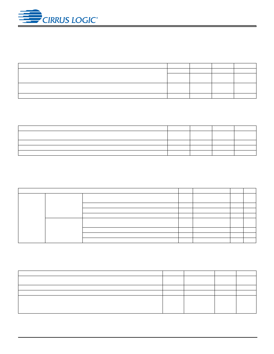
3 Characteristics and Specifications
3 Characteristics and Specifications
provides additional details about parameter definitions.
Table 3-1. Recommended Operating Conditions
Test conditions: GNDA = GNDD = 0 V; all voltages are with respect to ground.
Parameters
1
1.Device functional operation is guaranteed within these limits; operation outside them is not guaranteed or implied and may reduce device reliability.
Symbol
Min Max
Unit
DC power supply
Analog/Digital
VA
1.71
1.89
V
VP_MIN = 1
VP_MIN = 0
VP
3.2
3.0
5.25
5.25
V
V
External voltage applied to pin
2
2.The maximum over/under voltage is limited by the input current.
VA domain pins
V
IN-AI
–0.3
VA + 0.3
V
VP domain pins
V
IN-PI
–0.3
VP + 0.3
V
Ambient temperature
Commercial
T
A
–10
+70
C
Table 3-2. Absolute Maximum Ratings
Test conditions: GNDA = GNDD = 0 V; all voltages are with respect to ground.
Parameters
Symbol
Min
Max
Units
DC power supply
Analog/digital
Mic bias
VA
VP
–0.3
–0.3
2.22
5.6
V
V
Input current
1
1.Any pin except supplies. Transient currents of up to ±100 mA on the capture-path pins do not cause SCR latch-up.
I
in
—
±10
mA
Ambient operating temperature (power applied)
T
A
–50
+115
°C
Storage temperature (no power applied)
T
stg
–65
+150
°C
CAUTION: Operation at or beyond these limits may permanently damage the device.
Table 3-3. Combined ADC On-Chip Analog, Digital Filter, SRC, and DMIC Characteristics
Test conditions (unless otherwise specified): T
A
= +25°C; MCLK = 12.288 MHz; characteristics do not include the effects of external AC-coupling
capacitors. Path is INx to SDOUT. Analog and digital gains are all set to 0 dB; HPF disabled.
Parameters
1
1.Specifications are normalized to Fs and can be denormalized by multiplying by Fs.
Min
Typ
Max
Units
Fs
int
= Fs
ext
=
Fs = 48 kHz
[
2
]
2.See
for information about combined filter response when Fs
int
is not equal to Fs
ext
.
ADC notch filter on
(ADCx_NOTCH_
DIS = 0)
Passband
–0.05-dB corner
–3.0-dB corner
—
—
0.391
0.410
—
—
Fs
Fs
Passband ripple (0
Hz to 0.394 Fs; normalized to 0 Hz)
–0.13
—
0.14
dB
Stopband @ –70 dB
—
0.492
—
Fs
Total group delay
—
15.3/Fs
int
+ 6.5/Fs
ext
—
s
ADC notch filter off
(ADCx_NOTCH_
DIS = 1)
Passband
–0.05-dB corner
–3.0-dB corner
—
—
0.445
0.470
—
—
Fs
Fs
Passband ripple (0
Hz to 0.447 Fs; normalized to 0 Hz)
–0.09
—
0.14
dB
Stopband @ –70 dB
—
0.639
—
Fs
Total group delay
—
15.5/Fs
int
+ 6.6/Fs
ext
—
s
Table 3-4. ADC High-Pass Filter (HPF) Characteristics
Test conditions (unless specified otherwise): Analog and digital gains are all set to 0 dB; ADCx_HPF_CF = 00.
Parameters
1
1.Response scales with Fs
int
. Specifications are normalized to Fs
int
and are denormalized by multiplying by Fs
int
.
Min
Typ
Max
Units
Passband
2
2.Characteristics do not include effects of the analog HPF filter formed by the external AC-coupling capacitors and the input impedance.
–0.05-dB corner
–3.0-dB corner
—
—
3.57x10
–4
3.88x10
–5
—
—
Fs
int
Fs
int
Passband ripple (0.417x10
–3
Fs to 0.417 Fs; normalized to 0.417
Fs)
—
—
0.01
dB
Phase deviation @ 0.453 x 10
–3
Fs
—
4.896
—
°
Filter settling time
3
3.Required time for the magnitude of the DC component present at the output of the HPF to reach 5% of the applied DC signal.
ADCx_HPF_CF = 00 (3.88 x 10
–5
x Fs
int
mode)
ADCx_HPF_CF = 01 (2.5 x 10
–3
x Fs
int
mode)
ADCx_HPF_CF = 10 (4.9 x 10
–3
x Fs
int
mode)
ADCx_HPF_CF = 11 (9.7 x 10
–3
x Fs
int
mode)
—
—
—
—
12260/Fs
int
200/Fs
int
100/Fs
int
50/Fs
int
—
—
—
—
s
s
s
s