2 qfn, 3 pin descriptions, 2 qfn 1.3 pin descriptions – Cirrus Logic CS53L30 User Manual
Page 5: In1+/dmic1, In3+/dmic2, Cs53l30, Thermal pad
DS992F1
5
CS53L30
1.2 QFN
1.2 QFN
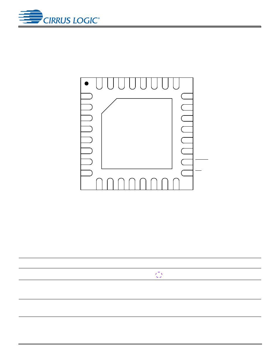
Figure 1-2. Top-Down (Through-Package) View—32-Pin QFN Package
1.3 Pin
Descriptions
Table 1-1. Pin Descriptions
Name
Ball
#
Pin
#
Power
Supply
I/O
Description
Internal
Connection
Driver
Receiver
State at
Reset
IN1+/DMIC1_SD
IN2+
IN3+/DMIC2_SD
IN4+
31
1
3
5
VA
I
Noninverting Inputs/DMIC Inputs.
Positive analog inputs for the stereo
ADCs when CH_TYPE = 0 (default) or
DMIC inputs when CH_TYPE = 1.
Programmable
—
Hysteresis
on CMOS
input
—
IN1–
IN2–
IN3–
IN4–
32
2
4
6
VA
I
Inverting Inputs. Negative analog inputs
for the stereo ADCs when CH_TYPE = 0
(default) or unused when CH_TYPE = 1.
Programmable
—
Hysteresis
on CMOS
input
—
Thermal Pad
10
9
8
7
6
5
4
3
2
1
11
12
13
14
15
16
17
18
19
20
21
22
23
24
25
26
27
28
29
30
31
32
Capture-Path Pins