Note 1, Note 3, Note 2 – Cirrus Logic CS53L30 User Manual
Page 8: Note 5, Note 4, Note 7, Note 6, Cs53l30, 2 typical connection diagram
8
DS992F1
CS53L30
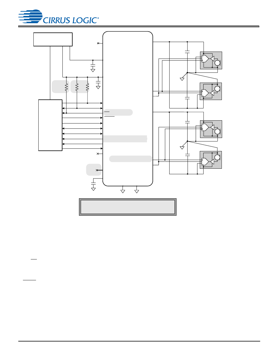
2 Typical Connection Diagram
Figure 2-2. Typical Connection Diagram—Digital Microphone Connections
1. The MICx_BIAS compensation capacitor must be 1 µF (nominal values indicated, can vary from the nominal by ±20%). This value is bounded
by the stability of the amplifier and the maximum rise-time specification of the output.
2. The DC-blocking capacitor, C
INM
, forms a high-pass filter whose corner frequency is determined by the capacitor value and the input
impedance. See
and
.
3. The reference terminal of the INx inputs connects to the ground pin of the mic cartridge in the pseudodifferential case. In a fully differential
configuration, the reference terminal of the INx inputs connects to the inverting output terminal of differential mic.
4. R
P_I
and R
P
can be calculated by using the values in
.
5. The value of R
BIAS
, the bias resistor for electret condenser mics, is dictated by the mic cartridge.
6. The INT pin is provided only on the QFN package.
7. ASP_SDOUT2/AD0 and DMIC2_SCLK/AD1 have internal pull-downs that allow for the default I
2
C address with no external components.
See
for typical and maximum pull-down values. If an I
2
C physical address other than the default is desired, then external resistor
termination to VA is required. The minimum value resistor allowed on these I/O pins is 10 k
The time constant resulting from the pull-up/
pull-down resistor and the total net capacitance should be considered when determining the time required for the pin voltage to settle before
RESET
is deasserted.
8. Unconnected INx pins can be terminated with an internal weak_vcm or weak pull-down by setting the termination in the INxy_BIAS bits. See
, and
CS53L30
GNDD
GNDA
Left Digital
Microphone 1
Right Digital
Microphone 1
IN1+/DMIC1_SD
DMIC1_SCLK
L /R
DATA
L/ R
DATA
IN3+/DMIC2_SD
Left Digital
Microphone 2
Right Digital
Microphone 2
L /R
DATA
L/ R
DATA
+1.8 V
+1.8 V
VP
0.1 µF
*
+3.6 V
FILT+
MIC_BIAS_FILT
*
4.7 µF
PMU
SCL
SDA
SoC
VA
0.1 µF
R
P
*
R
P
ASP_LRCK/FSYNC
ASP_SCLK
ASP_SDOUT1
MCLK
RESET
MUTE
R
P_ I
Key for Capacitor Types Required
:
*
Use low ESR, X7 R/X5R capacitors
All External Passive Component Values Shown Are Nominal Values
.
0.47 µF
0.47 µF
0.47 µF
0.47 µF
MIC1_BIAS
MIC3_BIAS
DMIC2_SCLK/AD1
SYNC
IN1
–
, IN2+, IN2
–
,
IN3
–
, IN4+, IN4
–
ASP_SDOUT2/AD0
INT