4 functional description, 1 overview, Cs53l30 – Cirrus Logic CS53L30 User Manual
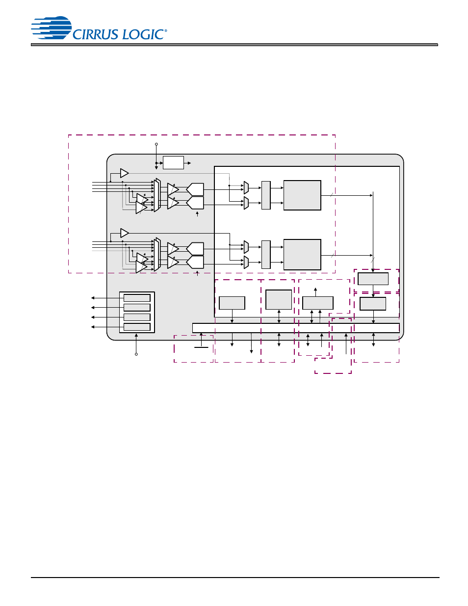
Page 18: Figure 4-1. overview of signal flow
18
DS992F1
CS53L30
4 Functional Description
4 Functional Description
This section provides a general description of the CS53L30 architecture and detailed functional descriptions of the various
blocks that comprise the CS53L30.
4.1 Overview
is a block diagram of the CS53L30 with links to descriptions of major subblocks.
Figure 4-1. Overview of Signal Flow
The CS53L30 is a low-power, four-channel, 24-bit audio ADC. The ADCs are fed by fully differential analog inputs that
support mic and line-level input signals. The ADCs are designed using multibit delta-sigma techniques. The ADCs operate
at an optimal oversampling ratio balancing performance with power savings. Enhanced power savings are possible when
the internal MCLK is scaled by setting
(see
lists supported sample rates with scaled
internal MCLK.
The serial data port operates at a selectable range of standard audio sample rates as either timing master or slave. Core
timing is flexibly sourced, without the need of a PLL, by clocks with typical audio clock rates (N x 5.6448, or N x 6.1440
MHz; where N = 1 or 2), USB rates (6 or 12 MHz), or 3G and DVB rates (19.2 MHz).
The integrated LDO regulator allows the digital core to operate at a very low voltage, significantly reducing the CS53L30’s
overall power consumption.
The CS53L30 can operate in a system with multiple CS53L30s to increase the number of channels available. The
CS53L30s may be connected in a multidrop configuration in TDM Mode. Up to four CS53L30s can operate simultaneously
on the same TDM bus. Connecting together the SYNC pins of multiple CS53L30s allows operation with minimal
channel-to-channel phase mismatch across devices.
The signal to be converted can be either mic/line-level. The digital mic inputs (IN1+/DMIC1_SD, IN3+/DMIC2_SD) connect
directly to the decimators.
CS53L30
Digital Processing
Control
Port
Level Shifters
MIC 1_BIAS
Serial Port
MIC 2_BIAS
VP
MCLK
DMIC1_SCLK
MIC3_BIAS
MIC4_BIAS
–6 to +12 dB,
0.5 dB steps
+10 or +20 dB
ADC1B
–
+
–
+
De
ci
ma
to
rs
–6 to +12 dB,
0.5 dB steps
+10 or +20 dB
–
+
–
+
De
cim
at
or
s
MIC1 Bias
MIC2 Bias
MIC3 Bias
MIC4 Bias
HPF, Noise
Gate, Volume,
Mute
Audio
Serial Port
Control Port
RESET
MCLK_INT
Clock Divider
Synchronizer
DMIC
ADC1A
ADC2B
ADC2A
–
+
–
+
LDO
VA
VD
2
2
4
MCLK_INT
MCLK_INT
HPF, Noise
Gate, Volume,
Mute
SYNC
MUTE
Synchronous
SRC
IN1+/DMIC1_SD
IN2–
IN1–
IN2+
IN3+/DMIC2_SD
IN4–
IN3–
IN4+
DMIC2_SCLK
See
See
.
.
See
See
.
See
See
.
See