Are shown in, Fig. 4-18, Cs53l30 – Cirrus Logic CS53L30 User Manual
Page 36: 14 i, C address with no external components. if an i, And v
36
DS992F1
CS53L30
4.14 I
2
C Control Port
AD0 and AD1 are the logic state of the ASP_SDOUT2/AD0 and DMIC2_SCLK/AD1 pins, which are pulled to the supply
or ground. These pins configure the I²C device address upon a device power up, after RESET is deasserted. These pins
have internal pull-down resistors, allowing for the default I
2
C address with no external components. If an I
2
C address other
than the default is desired, then external resistor termination to VA is required. The minimum resistor value allowed is 10
k
. The time constant resulting from the pull-up or pull-down resistor and the total net capacitance should be considered
when determining the time required for the pin voltage to settle before RESET is deasserted. See
specifications on internal pull-down resistance and V
IH
and V
IL
voltage.
The next byte is the memory address pointer (MAP); the 7 LSBs of the MAP byte select the address of the register to be
read or written to next. The MSB of the MAP byte, INCR, selects whether autoincrementing is to be used (INCR = 1),
allowing successive reads or writes of consecutive registers.
Each byte is separated by an acknowledge bit. The ACK bit is output from the CS53L30 after each input byte is read and
is input to the CS53L30 from the microcontroller after each transmitted byte.
If the operation is a write, the bytes following the MAP byte are written to the CS53L30 register address indicated by the
sum of the last-received MAP and the number of times the MAP has automatically incremented since the MAP was last
received.
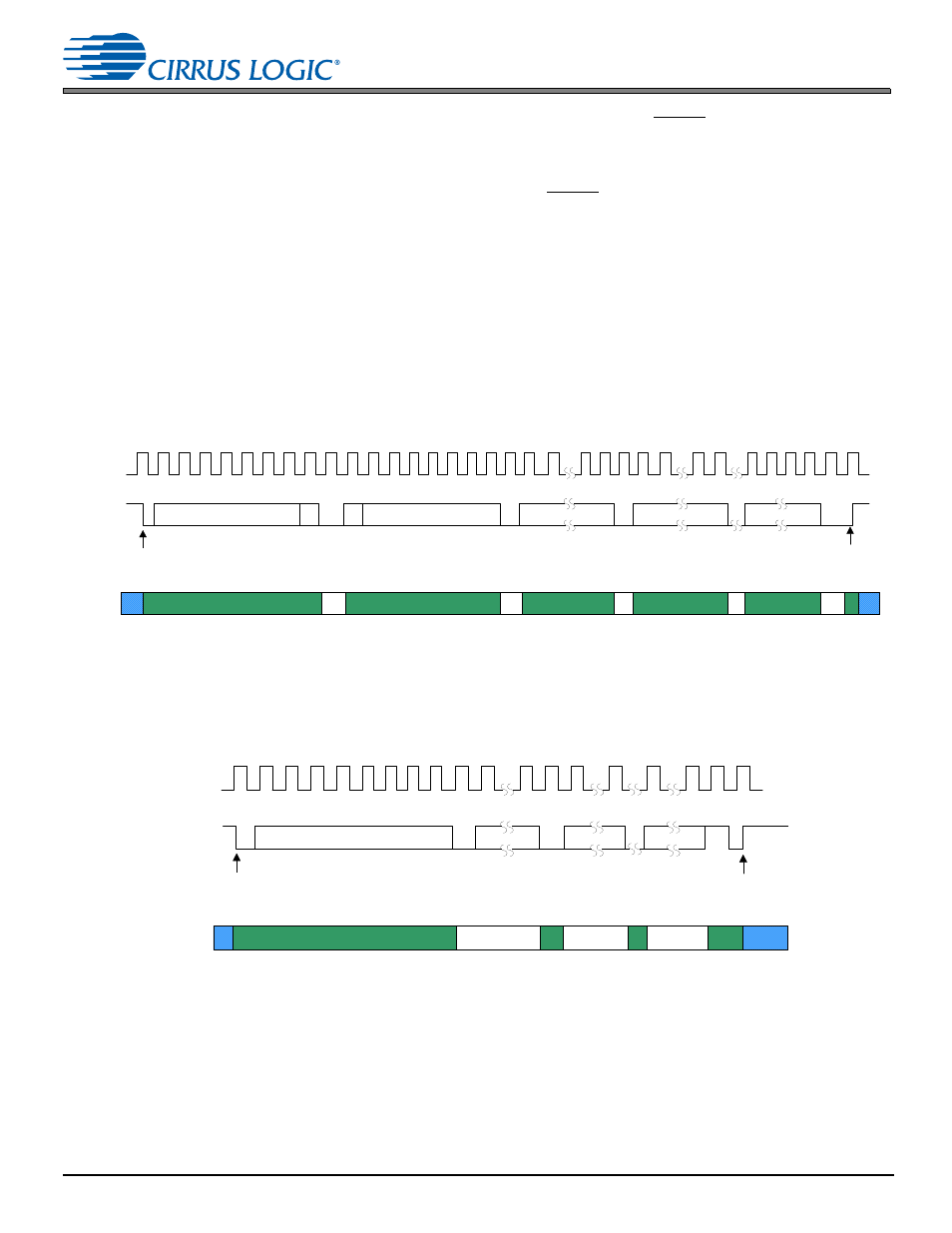
shows a write pattern with autoincrementing.
Figure 4-18. Control Port Timing, I
2
C Writes with Autoincrement
If the operation is a read, the contents of the register indicated by the sum of the last-received MAP and the number of
times the MAP has automatically incremented since it was last received, are output in the next byte.
shows a
read pattern following the write pattern in
. Notice how read addresses are based on the MAP byte from
.
Figure 4-19. Control Port Timing, I
2
C Reads with Autoincrement
If a read address not based on the last received MAP address is desired, an aborted write operation can be used as a
preamble that sets the desired read address. This preamble technique is shown in
: A write operation is aborted
(after the acknowledge for the MAP byte) by sending a stop condition.
4 5 6 7
24 25
SCL
Chip Address (Write)
MAP Byte
Data
Data
START
STOP
ACK
ACK
SDA
0 1 2 3
8 9
12
16 17 18 19
10 11
13 14 15
27 28
26
Data
SDA
Source
Master
Master
Master
Pullup
Slave
Slave
Slave
Slave
Master
Pullup
ACK
ACK
MAP Addr = X
INCR
=
1
R/
W
=
0
D
a
ta
t
o
Ad
d
r X+
1
D
a
ta
t
o
Ad
d
r X+
n
Master
Master
Slave
D
a
ta
t
o
Ad
d
r X
Addr = 1001010
6
4
3
2
5
7
1
0
6
4
3
2
5
7
1
0
6
7
1
0
6
7
1
0
6
7
1 0
SCL
SDA
SDA
Source
Pullup
DATA
STOP
ACK
ACK
CHIP ADDRESS (READ)
START
NO
25
8 9
18
4 5 6 7
0 1 2 3
16 17
34 35 36
ACK
R/W
=
1
DATA
DATA
D
a
ta
f
ro
m
Ad
d
r X+n
+
1
D
a
ta
f
ro
m
Ad
d
r X+n
+
2
D
a
ta
f
ro
m
Ad
d
r X+n
+
3
Master
Slave
Slave
Slave
Master
Master
Master
Pullup
27
Addr = 1001010
6
4
3
2
5
7
1
0
7
0
7
0
7
0