Table 3-11. specifications—i2s, Specifications—i, Cs53l30 – Cirrus Logic CS53L30 User Manual
Page 14
14
DS992F1
CS53L30
3 Characteristics and Specifications
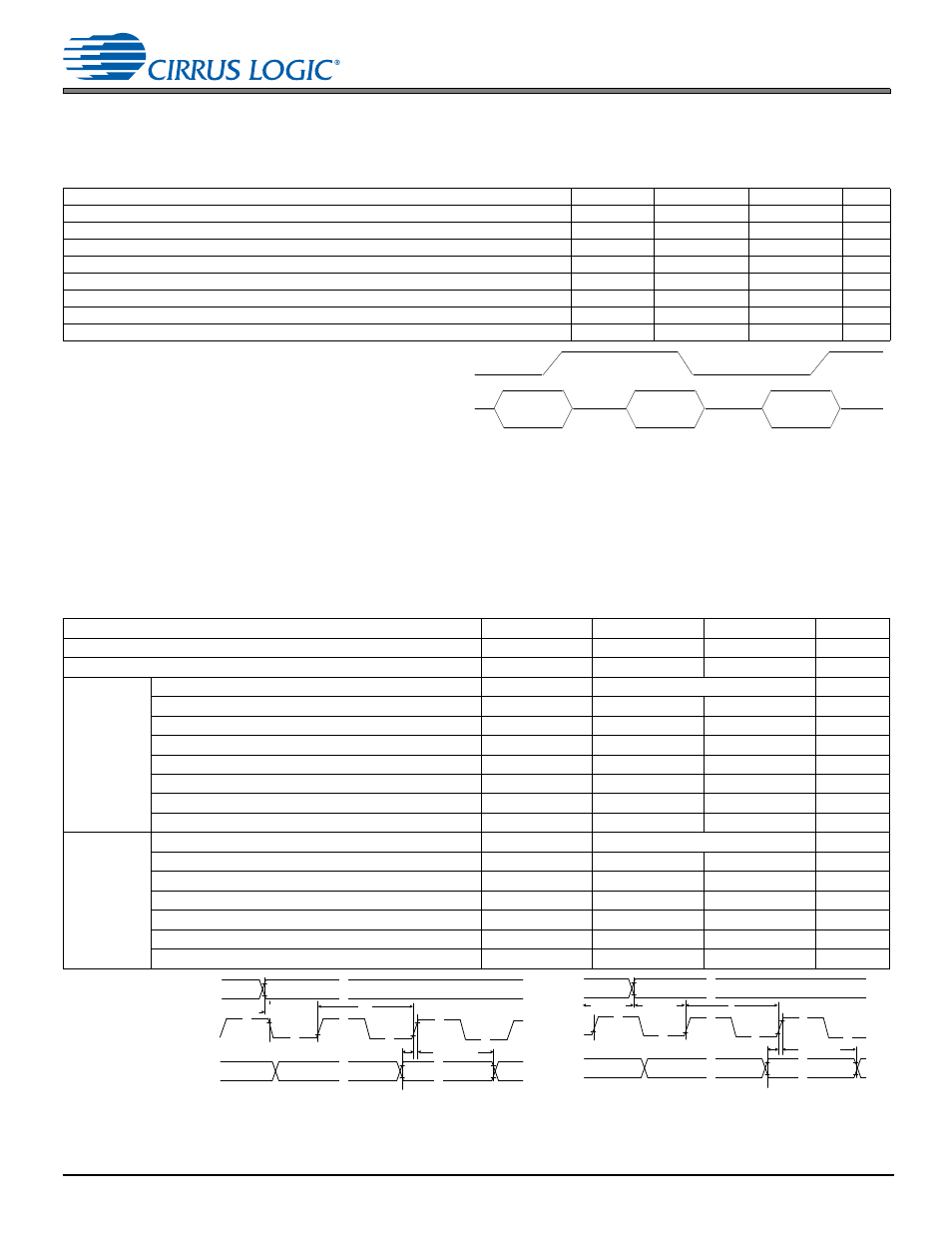
Table 3-10. Switching Specifications—Digital Mic Interface
Test conditions (unless specified otherwise):
shows CS53L30 connections; GNDA = GNDD = 0 V; voltages are with respect to ground;
parameters can vary with VA, typical performance data taken with VA = 1.8 V, VP = 3.6 V, min/max performance data taken with VA = 1.8 V, VP = 3.6 V;
T
A
= +25°C; logic 0 = ground, logic 1 = VA; DMIC_DRIVE = 0 (normal); input timings are measured at V
IL
and V
IH
thresholds, and output timings are
measured at V
OL
and V
OH
thresholds (see
Parameters
1,2
1.Digital mic interface timing
2.Oversampling rate of the digital mic must match the oversampling rate of the CS53L30 internal decimators.
Symbol Min
Max
Units
Output clock (DMICx_SCLK) frequency
1/t
P
—
3.2
[3]
3.The output clock frequency follows the internal MCLK rate divided by 2 or 4, as set in the ADCx/DMICx control registers (see
on
). DMICx_SCLK is further divided by up to a factor of 4 when
). MCLK
source deviation from nominal supported rates is applied directly to the output clock rate by the same factor (e.g., a +100-ppm offset in the frequency
of MCLK becomes a +100-ppm offset of DMICx_SCLK.
MHz
DMICx_SCLK duty cycle
—
45
55
%
DMICx_SCLK rise time (10% to 90% of VA)
4
4.Timing guaranteed with pull-up or pull-down resistor, with a minimum value 10 k
tied to DMIC2_SCLK/AD1 for I
2
C address determination.
t
r
—
21
ns
DMICx_SCLK fall time (90% to 10% of VA)
t
f
—
13
ns
DMICx_SD setup time before DMICx_SCLK rising edge
t
s(SD-CLKR)
10
—
ns
DMICx_SD hold time after DMICx_SCLK rising edge
t
h(CLKR-SD)
4
—
ns
DMICx_SD setup time before DMICx_SCLK falling edge
t
s(SD-CLKF)
10
—
ns
DMICx_SD hold time after DMICx_SCLK falling edge
t
h(CLKF-SD)
4
—
ns
Table 3-11. Specifications—I
2
S
Test conditions (unless specified otherwise):
shows CS53L30 connections; GNDA = GNDD = 0 V; all voltages are with respect to ground;
parameters can vary with VA; typical performance data taken with VA = 1.8 V, VP = 3.6 V; min/max performance data taken with VA = 1.8 V, VP = 3.6 V;
T
A
= +25°C; Test load for ASP_LRCK/FSYNC, ASP_SCLK, and ASP_SDOUTx C
L
= 60 pF; logic 0 = ground, logic 1 = VA; ASPx_DRIVE = 0; input
timings are measured at V
IL
and V
IH
thresholds, and output timings are measured at V
OL
and V
OH
thresholds (see
).
Parameters
1,2
1.Serial port
interface timing
2.MCLK must be stable before powering up the device. In Slave Mode, ASP_LRCK/FSYNC and ASP_SCLK must be stable before powering up the
device. Before making changes to any clock setting, the device must be powered down by setting either the PDN_ULP or PDN_LP bit.
Symbol
Min Max
Units
MCLK frequency
—
1.024
19.2
MHz
MCLK duty cycle
—
45
55
%
Slave mode
Input sample rate (LRCK)
Fs
(See
)
kHz
LRCK duty cycle
—
45
55
%
SCLK frequency
1/t
Ps
—
64•Fs
ext
Hz
SCLK duty cycle
—
45
55
%
SCLK rising edge to LRCK edge
t
hs(LK-SK)
10
—
ns
LRCK setup time before SCLK rising edge
t
ss(LK-SK)
40
—
ns
SDOUT setup time before SCLK rising edge
t
ss(SDO-SK)
20
—
ns
SDOUT hold time after SCLK rising edge
t
hs(SK-SDO)
30
—
ns
Master mode Output sample rate (LRCK) All speed modes
Fs
ext
(See
)
kHz
LRCK duty cycle
—
45
55
%
SCLK frequency
1/t
Pm
—
64•Fs
ext
Hz
SCLK duty cycle
—
33
67
%
LRCK time before SCLK falling edge
t
sm(LK-SK)
–2
+2
ns
SDOUT setup time before SCLK rising edge
t
sm(SDO-SK)
20
—
ns
SDOUT hold time after SCLK rising edge
t
hm(SK-SDO)
30
—
ns
DMIC_CLK
DMIC_SD
Left
(A, DATA1 )
Channel Data
Right
(B , DATA2)
Channel Data
Left
(A, DATA1)
Channel Data
t
hm(SK-SDO)
//
//
//
//
//
//
MSB
LRCK
SCLK
SDOUT
t
Pm
t
sm(SDO-SK)
//
//
//
//
//
//
t
sm(LK-SK)
t
hs(SK-SDO)
//
//
//
//
//
//
MSB
LRCK
SCLK
SDOUT
t
ss(LK-SK)
t
P
t
ss(SDO-SK)
//
//
//
//
//
//
t
hs(LK-SK)
Serial Port Timing—Master Mode
Serial Port Timing—Slave Mode