Switching specifications—i, Cs53l30 – Cirrus Logic CS53L30 User Manual
Page 16

16
DS992F1
CS53L30
3 Characteristics and Specifications
8.Hand-off timing for multidevice
systems (SHIFT_LEFT = 1).
When
= 1, it is
recommended to insert an empty
slot between devices on the
TDM bus to prevent contention
possibilities.
9.In Master Mode, the output sample rate follows the MCLK rate, per
. MCLK deviations from the nominal supported rates are passed
directly to the output sample rate by the same factor (e.g., a +100 ppm offset in the frequency of MCLK becomes a +100 ppm offset in FSYNC).
10.“n” refers to number of SCLK cycles programmed in
(see
) when
) is set;
otherwise, t
FSYNC
has a 50% duty cycle.
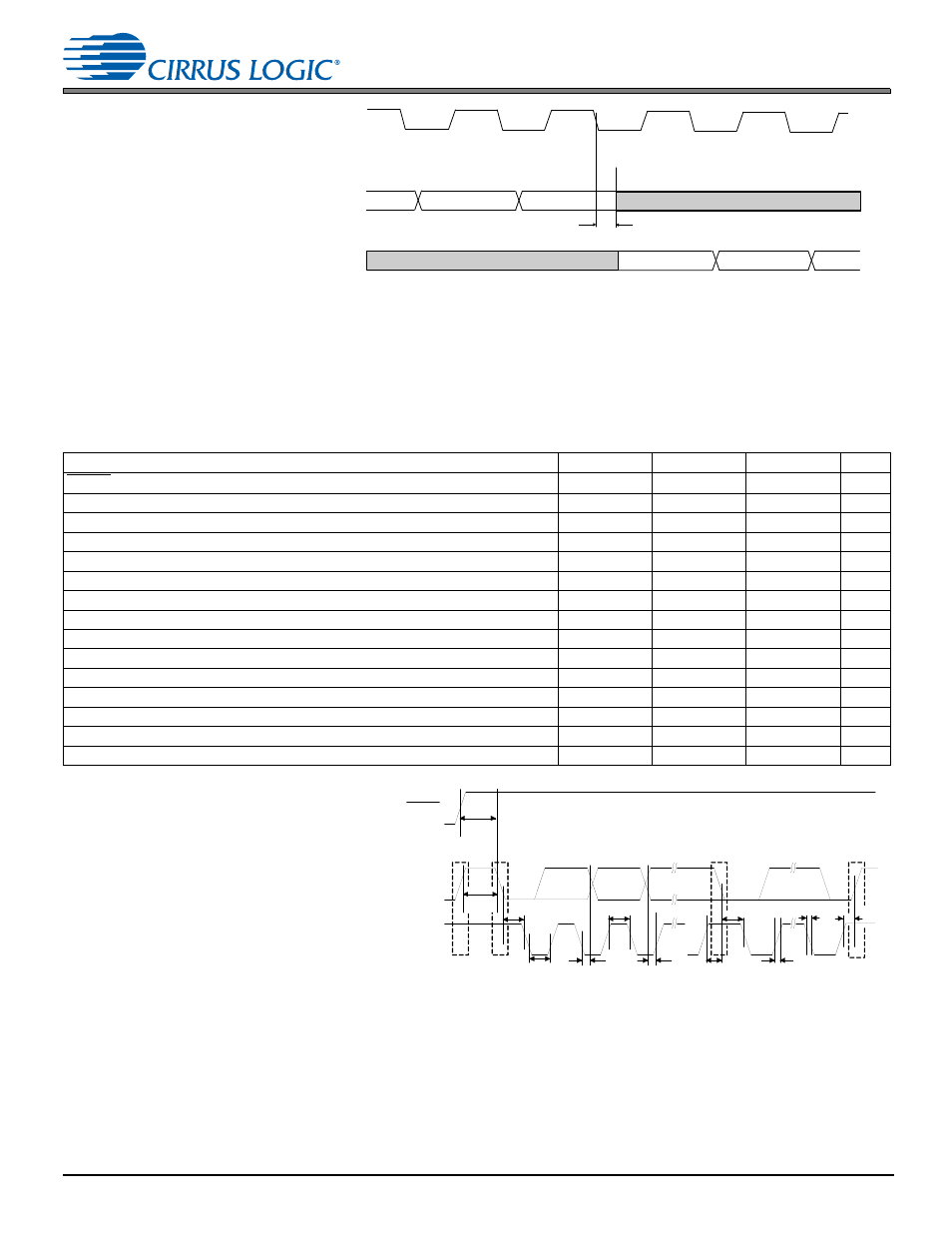
Table 3-13. Switching Specifications—I
2
C Control Port
Test conditions (unless specified otherwise):
shows CS53L30 connections; GNDA = GNDD = 0 V; all voltages are with respect to ground;
Parameters can vary with VA, typical performance data taken with VA = 1.8 V, VP = 3.6 V, min/max performance data taken with VA = 1.8 V, VP = 3.6 V;
T
A
= +25°C; logic 0 = ground, logic 1 = VA; input timings are measured at V
IL
and V
IH
thresholds, and output timings are measured at V
OL
and V
OH
thresholds (see
Parameter
1,2
1.All specifications are valid for the signals at the pins of the CS53L30 with the specified load capacitance.
2.I
2
C control port timing.
Symbol
Min
Max
Unit
RESET rising edge to start
t
irs
500
—
ns
SCL clock frequency
f
scl
—
550
kHz
Start condition hold time (prior to first clock pulse)
t
hdst
0.6
—
µs
Clock low time
t
low
1.3
—
µs
Clock high time
t
high
0.6
—
µs
Setup time for repeated start condition
t
sust
0.6
—
µs
SDA input hold time from SCL falling
3
3.Data must be held for sufficient time to bridge the transition time, t
f
, of SCL.
t
hddi
0
0.9
µs
SDA output hold time from SCL falling
t
hddo
0.2
0.9
µs
SDA setup time to SCL rising
t
sud
100
—
ns
Rise time of SCL and SDA
t
rc
—
300
ns
Fall time SCL and SDA
t
fc
—
300
ns
Setup time for stop condition
t
susp
0.6
—
µs
Bus free time between transmissions
t
buf
1.3
—
µs
SDA bus capacitance
C
L
—
400
pF
SDA pull-up resistance
R
p
500
—
SLOTx:LSB+1
SCLK
Device 0: SDOUT
t
HOLD2
SLOTx:LSB
SLOTx:MSB
SLOTx:MSB -1
SLOTx:MSB -2
Output Not Driven (Hi-Z)
Output Not Driven (Hi-Z)
t
buf
t
hdst
t
hdst
t
low
t r
t f
t
hdd
t high
t sud
t sust
t susp
Stop
Start
Start
Stop
Repeated
SDA
SCL
t
irs
RESET
