Section 5.4.1.2, Fig. 5-2, Fig. 5-3 – Cirrus Logic CS53L30 User Manual
Page 43: Cs53l30, 2 adc fullscale input level, 4 capture-path inputs, Actually delivers a 2•vx v
DS992F1
43
CS53L30
5.4 Capture-Path Inputs
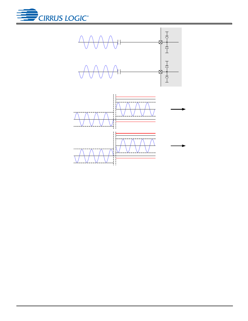
Figure 5-2. Differential Analog Input Signal to IN±, with Protection Diodes Shown
Figure 5-3. Differential Analog Input Signal to IN±, Voltage-Level Details Shown
, it is worth noting that a differential analog signal of 4•Vx V
PP
actually delivers a 2•Vx V
PP
signal
centered around VA/2 at each of the analog pin pairs. Thus, the signal peak (at the pin) of Vx + VA/2 should not exceed
VA + 0.3 V; the signal trough of –Vx + VA/2 (at the pin) should not be lower than GNDA – 0.3 V.
Although it is safe to use an input signal with resulting peak up to VA + 0.3 V and trough of GNDA – 0.3 V at the pin, signal
distortion at these maximum levels may be significant. This is caused by the onset of conduction of the protection diodes.
It is recommended that capture-path pin voltages stay between GNDA and VA to avoid signal distortion and clipping from
the slightly conductive state of protection diodes in the VA to VA + 0.3-V region and GNDA – 0.3-V to GNDA region.
5.4.1.2 ADC Fullscale Input Level
If the signal peaks are kept below the protection diode turn-on region per instructions in
, the maximum
capture-path signal level becomes solely a function of the applied analog gain, with the ADC fullscale input level being
constant, hard limit for the path.
shows all analog gain blocks in the analog signal path in relation to the input pin
and ADC. All signals levels mentioned refer to differential signals in V
PP
.
For any given input pin pairs (INx±), the product of the signal level at those input pins and the total analog gain must be
less than the ADC fullscale input level, i.e.,
By rearranging terms, substituting register bit names for the analog gain stages, the following inequality is obtained:
The ADC fullscale input level is specified in
. PREAMPx and PGAxVOL refer to the dB values set by the
respective register bits.
IN+
IN–
4Vx Vpp Differential signal
GNDA
+Vx
–Vx
GNDA
+Vx
–Vx
VA
GNDA
VA
GNDA
GNDA
GNDA
+Vx
–Vx
VA/2
Vx + VA/2
–Vx + VA/2
GNDA
GNDA
+Vx
–Vx
VA/2
Vx + VA/2
–Vx + VA/2
To IN+
To IN–
VA
VA + 0.3
GNDA – 0.3
VA
VA + 0.3
GNDA – 0.3
4Vx Vpp Differential signal
D
C
bl
oc
k
ing c
apac
it
or
D
C
bl
oc
ki
ng c
apac
it
or
Input Signal Level
Preamp and PGA gain
ADC Fullscale Input Level
Input Signal Level
10
PREAMPx
PGAxVOL
+
20
--------------------------------------------------------------------
–
0.82
VA