3 bdi port, 3 bdi port -3, Figure 5-1. dai port block diagram -3 – Cirrus Logic CS4953xx User Manual
Page 59
5-3
Copyright 2010 Cirrus Logic, Inc.
DS732UM10
Digital Audio Input Port Description
CS4953xx Hardware User’s Manual
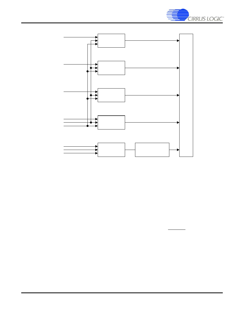
Figure 5-1. DAI Port Block Diagram
Currently supported are 4 lines of linear PCM input (DAI_DATA[3:0]) and 1 line of compressed audio or
linear PCM (DAI_DATA4). These two inputs can have their own clock domains. The firmware currently
available can operate on only one of these inputs at a time, providing for compressed data decode, stereo
PCM processing, or multichannel PCM processing. Please see AN288, “CS4953xx Firmware User’s
Manual” for details about configuring the firmware to select these different inputs to process.
5.1.3 BDI Port
Note: Currently not supported in the O/S.
The Bursty Data Input (BDI) port on the CS4953xx shares pins with the DAI port pins, and is used for
input of bursty compressed audio data. The compressed data is clocked in with a bit clock (BDI_CLK).
Bursty compressed audio data input requires the use of a “throttle” signal, BDI_REQ to signal to the host
that the CS4953xx is capable of accepting data.
shows the mnemonic and pin description of the
pins associated with the Bursty Data Input (BDI) port on CS4953xx.
DAI1_DATA0
D
M
A
to
Per
iph
era
l B
u
s
DAI_DATA0
DAI1_DATA1
DAI_DATA1
DAI1_DATA2
DAI_DATA2
DAI1_DATA3
DAI_DATA3
DAI2_DATA
or
DAI1_DATA4
DAI_DATA4
Compressed Data
Unit
DAI_LRCLK1
DAI_SCLK1
DAI_LRCLK2
DAI_SCLK2