Cirrus Logic CS4953xx User Manual
Page 113
D
S
73
2U
M
1
0
C
op
yri
ght 201
0
C
irr
us Log
ic
,
In
c
9
-2
5
Pin A
s
s
ign
me
nts
C
S
495
3xx
H
a
rd
w
a
re
U
s
e
r’s
M
a
n
ual
109
-
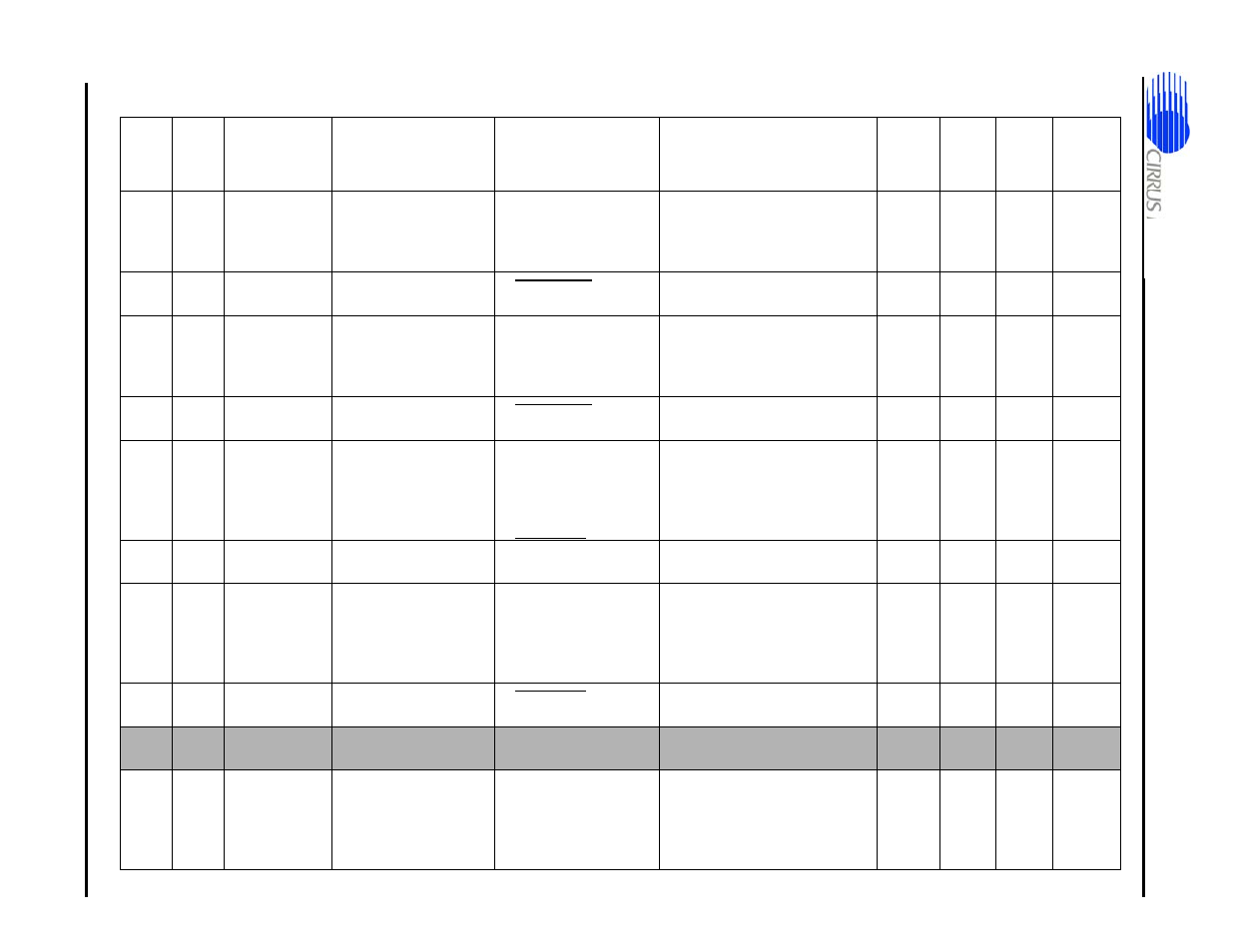
GPIO9
General Purpose
Input/Output
1. PCP_A1
2. PCP_A9
1. Parallel Control Port
Address Bit 1
2. Parallel Control Port
Address Bit 9
3.3V
(5V tol)
BiDir
IN
Y
-
4
GPIO9
General Purpose
Input/Output
1. SCP1_IRQ
1. Serial Control Port Data
Ready Interrupt Request
3.3V
(5V tol)
BiDir
IN
Y
110
-
GPIO8
General Purpose
Input/Output
1. PCP_A0
2. PCP_A8
1. Parallel Control Port
Address Bit 0
2. Parallel Control Port
Address Bit 8
3.3V
(5V tol)
BiDir
IN
Y
-
5
GPIO8
General Purpose
Input/Output
1. SCP2_IRQ
1. Serial Control Port Data
Ready Interrupt Request
3.3V
(5V tol)
BiDir
IN
Y
111
-
GPIO7
General Purpose
Input/Output
1. PCP_D7
2. PCP_AD7
1. Parallel Control Port Data
Bus
2. Parallel Control Port
Multiplexed Address and Data
Bus
3.3V
(5V tol)
BiDir
IN
Y
-
6
GPIO7
General Purpose
Input/Output
1. SCP1_CS
2. IOWAIT
1. SPI Chip Select
2. SRAM Hold-Off Handshake
3.3V
(5V tol)
BiDir
IN
Y
112
-
GPIO6
General Purpose
Input/Output
1. PCP_D6
2. PCP_AD6
1. Parallel Control Port Data
Bus
2. Parallel Control Port
Multiplexed Address and Data
Bus
3.3V
(5V tol)
BiDir
IN
Y
-
7
GPIO6
General Purpose
Input/Output
1. SCP2_CS
1. SPI Chip Select
3.3V
(5V tol)
BiDir
IN
Y
113
8
VDDIO7
I/O power supply
voltage
3.3V
PWR
114
-
GPIO5
General Purpose
Input/Output
1. PCP_D5
2. PCP_AD5
1. Parallel Control Port Data
Bus
2. Parallel Control Port
Multiplexed Address and Data
Bus
3.3V
(5V tol)
BiDir
IN
Y
Table 9-10. Pin Assignments (Continued)
LQFP-
144
Pin #
LQFP-
128
Pin #
Function 1
(Default)
Description of Default
Function
Secondary Functions
Description of Secondary
Functions
Pwr
Type
Reset
State
Pullup
at
Reset