Cs4953xx – Cirrus Logic CS4953xx User Manual
Page 10
Overview
CS4953xx Hardware User’s Manual
DS732UM10
Copyright 2010 Cirrus Logic, Inc
1-2
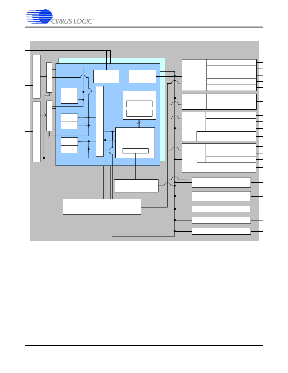
illustrates the functional block diagram for the CS4953xx chip.
Figure 1-1. CS4953xx Chip Functional Block Diagram
See AN288, “CS4953xx/CS497xxx for a list of audio decoding/processing algorithms that are supported
by the CS4953xx: These firmwware modules and their associated application notes are available through
the Cirrus Logic Software Licensing Program. .
The CS4953xx contains sufficient on-chip memory to support decoding of all major audio decoding
algorithms available today. The CS4953xx supports a glueless SDRAM/Flash interface for increased all-
channel delays. The memory interface also supports connection to an external 8- or 16-bit-wide EPROM
or Flash memory for code storage, thus allowing products to be field upgraded as new audio algorithms
are developed.
This chip, teamed with the Cirrus certified decoder library, Cirrus digital interface products, and mixed-
signal data converters, enables the design of next-generation digital entertainment products.
DAI
Controller
DMA Controller with 11 Stereo Channels
Programmable
Interrupt Controller
Peripheral
Bus
Controller
M
e
m
o
ry Cont
rol
le
r
Log/Exp
Security
Ext (64 bit)
DMA Bus
Peripheral Bus
Decryptor
32-bit Dual Datapath
DSP
with 72-bit
Accumulators
X
Y
P
X
P
Y
64 bit
Stereo Audio Output
Stereo Audio Output
Stereo Audio Output
Arb
ite
r
Ar
b
ite
r
Stereo Audio Output or
SPDIF Transm itter
DAO
Controller
ROM
SRAM
ROM
SRAM
ROM
SRAM
Timers
GPIOs
Clock Manager and PLL
Parallel Control Port
Serial Control Port
S
DRAM
C
o
nt
rol
le
r
SRA
M
/
F
L
ASH
C
o
n
tro
lle
r
Debug
Controller
DSPA
DSPB
DAO1
Stereo Audio Input/DSD
Stereo Audio Input/DSD
Stereo Audio Input/DSD
Stereo Audio Input/DSD
Stereo Audio Output
Stereo Audio Output
Stereo Audio Output
Stereo Audio Output or
SPDIF Transmitter
DAO
Controller
DAO2
DAI1
CS4953xx
Stereo Audio Input /
Bursty Data Input/DSD
Stereo Audio Input/DSD
DAI2
DAI
Controller