7 pin assignments, 7 pin assignments -17, Table 9-10. pin assignments -17 – Cirrus Logic CS4953xx User Manual
Page 105
D
S
73
2U
M
1
0
C
op
yri
ght 201
0
C
irr
us Log
ic
,
In
c
9
-1
7
Pin A
s
s
ign
me
nts
C
S
495
3xx
H
a
rd
w
a
re
U
s
e
r’s
M
a
n
ual
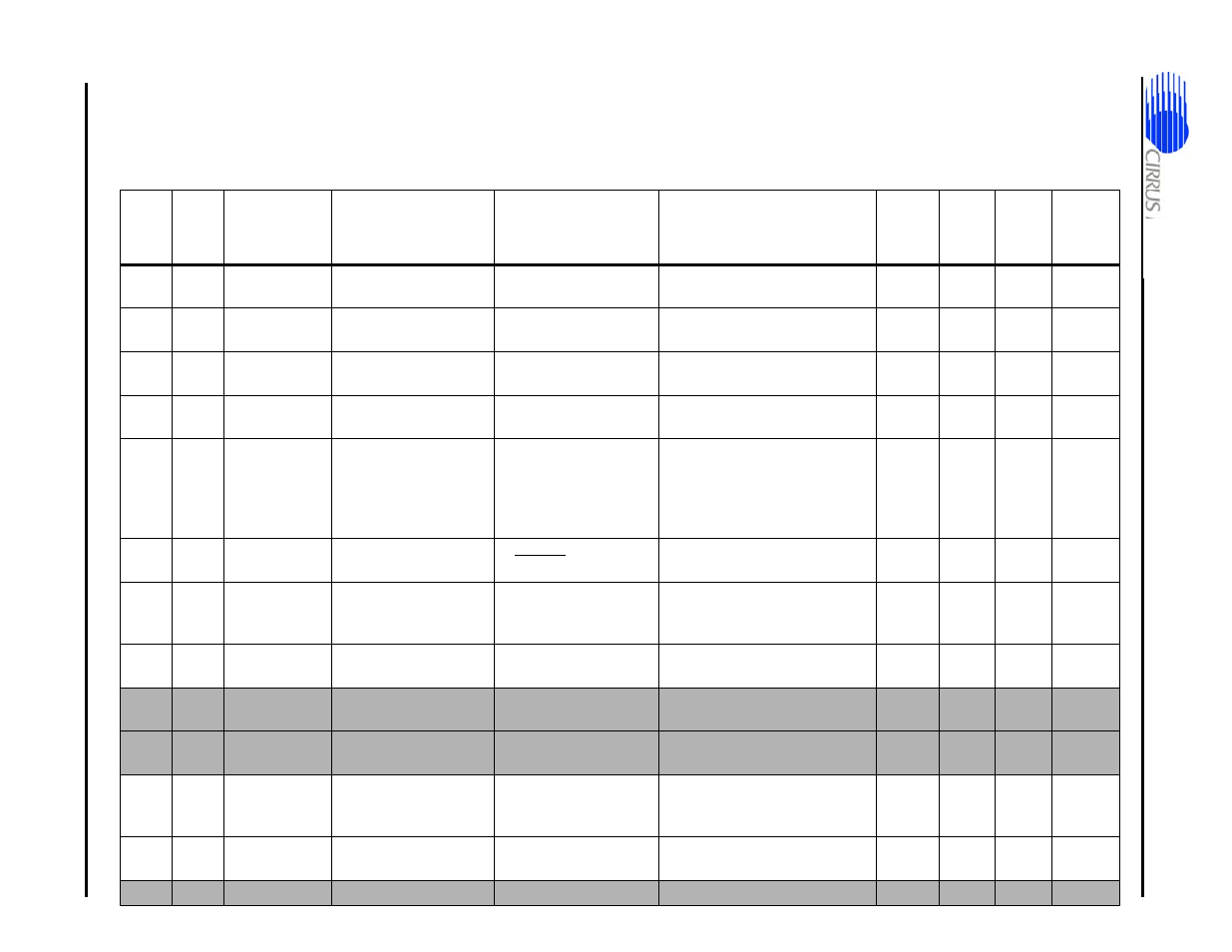
9.7 Pin Assignments
shows the names and functions for each pin.
Table 9-10. Pin Assignments
LQFP-
144
Pin #
LQFP-
128
Pin #
Function 1
(Default)
Description of Default
Function
Secondary Functions
Description of Secondary
Functions
Pwr
Type
Reset
State
Pullup
at
Reset
1
-
GPIO28
General Purpose
Input/Output
3.3V
(5V tol)
BiDir
IN
Y
2
-
GPIO29
General Purpose
Input/Output
1. XMTA_IN
1. S/PDIF Pass-thru Input.
3.3V
(5V tol)
BiDir
IN
Y
3
36
DBDA
Debug Data
3.3V
(5V tol)
In/OD
IN
Y
4
37
DBCK
Debug Clock
3.3V
(5V tol)
In/OD
IN
Y
5
-
GPIO21
General Purpose
Input/Output
1. DAO2_DATA3
2. XMTB
3. UART_TX_ENABLE
1. Digital Audio Output 3.
2. Outputs IEC60958/61937
format bi-phase mark encoded
S/PDIF data.
3. Enable the UART_TX pin.
3.3V
(5V tol
BiDir
IN
Y
6
38
GPIO20
General Purpose
Input/Output
1. DAO2_DATA2
2. EE_CS
1.Digital Audio Output 2.
2. EEPROM Boot Chip Select.
3.3V
(5V tol
BiDir
IN
Y
7
39
GPIO19
General Purpose
Input/Output
1. DAO2_DATA1
2. HS4
1. Digital Audio Output 1.
2. Hardware Strap Mode
Select.
3.3V
(5V tol)
BiDir
IN
Y
8
40
DAO_MCLK
Audio Master Clock
3.3V
(5V tol)
BiDir
IN
Y
9
41
TEST
Test
3.3V
(5V tol)
In
10
42
VDD1
Core power supply
voltage
1.8V
PWR
11
43
GPIO18
General Purpose
Input/Output
1. DAO2_DATA0
2. HS3
1. Digital Audio Output 0.
2. Hardware Strap Mode
Select.
3.3V
(5V tol)
BiDir
IN
Y
12
44
GPIO22
General Purpose
Input/Output
DAO2_SCLK
PCM Audio Bit Clock.
3.3V
(5V tol)
BiDir
IN
Y
13
45
GNDD1
Core ground
0V
PWR