6 scp1_irq behavior, 4 spi port, 4 spi port -13 – Cirrus Logic CS4953xx User Manual
Page 45
3-13
Copyright 2010 Cirrus Logic, Inc.
DS732UM10
SPI Port
CS4953xx Hardware User’s Manual
3.3.3.6 SCP1_IRQ Behavior
Once the BOOT_ASSIST_A (.ULD file) has been downloaded in accordance to Steps 1 through 8 in
Section 2.3.1 “Host Controlled Master Boot”
on page 4 or Steps 1 through 8 in
on page 7, the SCP1_IRQ pin is functionally enabled.
The SCP1_IRQ signal is not part of the I
2
C protocol, but is provided so that the slave can signal that it has
data to be read. A high-to-low transition on SCP1_IRQ indicates to the master that the slave has data to
be read. When a master detects a high-to-low transition on SCP1_IRQ, it should send a Start condition
and begin reading data from the slave.
SCP1_IRQ is guaranteed to remain low (once it has gone low), until the falling edge of SCP1_CLK for the
last bit of the last byte to be transferred out of CS4953xx (that is, the rising edge of SCP1_CLK before the
ACK). If there is no more data to be transferred, SCP1_IRQ will go high at this point. After going high,
SCP1_IRQ is guaranteed to stay high until the next rising edge of SCP1_CLK (that is, it will stay high until
the rising edge of SCP1_CLK for the ACK/NACK bit).
This end-of-transfer condition signals the master to end the read transaction by clocking the last data bit
out of CS4953xx and then sending a NACK to CS4953xx to signal that the read sequence is over. At this
point, the master should send an I
2
C
stop condition to complete the read sequence. If SCP1_IRQ is still
low after the rising edge of SCP1_CLK on the last data bit of the current byte, the master should send an
acknowledge and continue reading data from the serial control port. It should be noted that all data should
be read out of the serial control port during one cycle or a loss of data will occur. In other words, all data
should be read out of the chip until SCP1_IRQ signals the last byte by going high as described above.
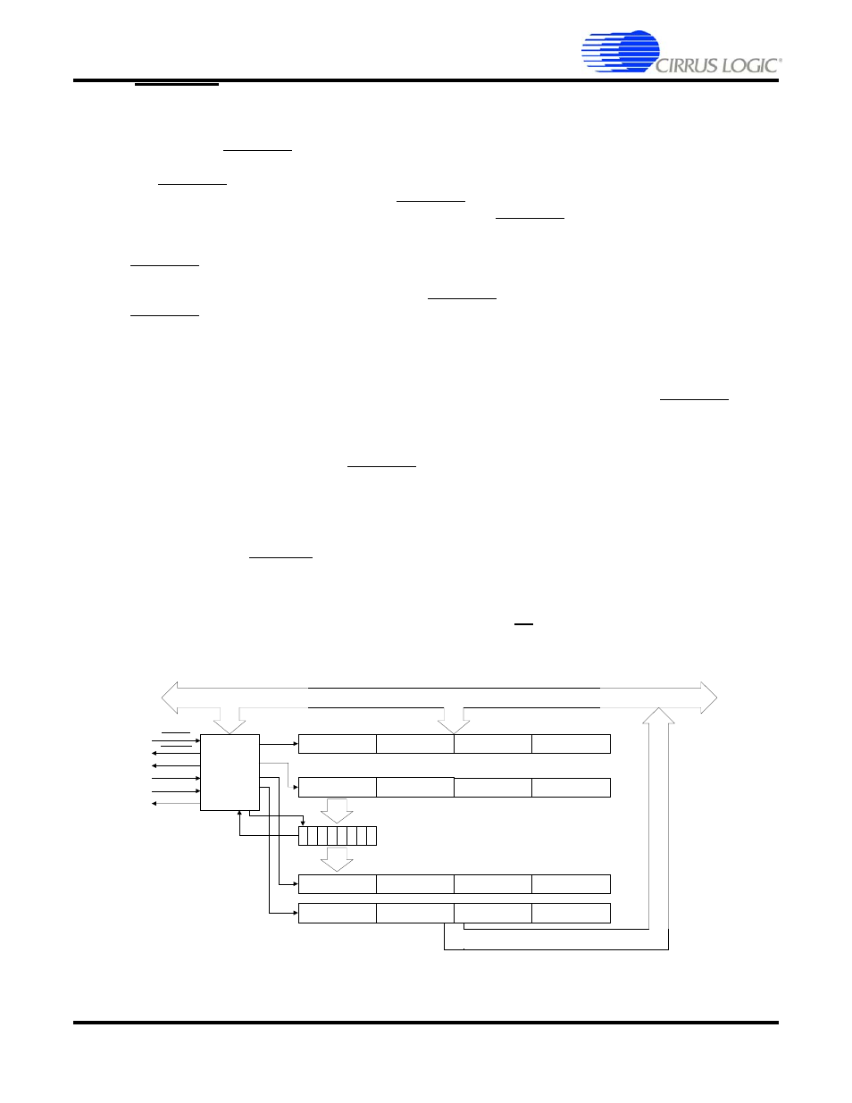
3.4 SPI Port
The CS4953xx Serial Peripheral Interface (SPI) bus has been developed for 8-bit digital control
applications, such as those requiring microcontrollers. SPI communication is accomplished with 5 lines:
Serial Chip Select (SCP1_CS), Serial Control Clock (SCP1_CLK), Master Out/Slave In data
(SCP1_MOSI), and a Master In/Slave Out data (SCP1_MISO). Although the separate data I/O lines
provide full-duplex capabilities, the CS4953xx chip only uses a half-duplex SPI-bus. Each device on the
bus may respond to one or more unique commands, and can operate as either a transmitter or receiver. A
device is considered the master in a transaction if it drives the CS pin of another device, and is also
mastering the SCP1_CLK line. A block diagram of the CS4953xx SPI Serial Control Port is provided in
Figure 3-12. SPI Serial Control Port Internal Block Diagram
SPI Control /
Clocking
SCP1_BSY
SCP1_IRQ
LSB (Byte 0)
Byte 1
Byte2
MSB (Byte 3)
LSB (Byte 0)
Byte 1
Byte2
MSB (Byte 3)
MSB (Byte 3)
Byte 2
Byte1
LSB (Byte 0)
MSB (Byte 3)
Byte 2
Byte1
LSB (Byte 0)
7
6
5
4
3
2
1
0
Internal Bus
SCP1_CLK
SCP1_MOSI
SCP1_MISO
SCP1_CS