Campbell Scientific CR10X Measurement and Control System User Manual
Page 148
SECTION 9. INPUT/OUTPUT INSTRUCTIONS
9-16
c
V
o s
Sensor
with
DC
offset
Silicon diodes
such as 1N4001
To single - ended
input
1µF
D1
D2
R
10k
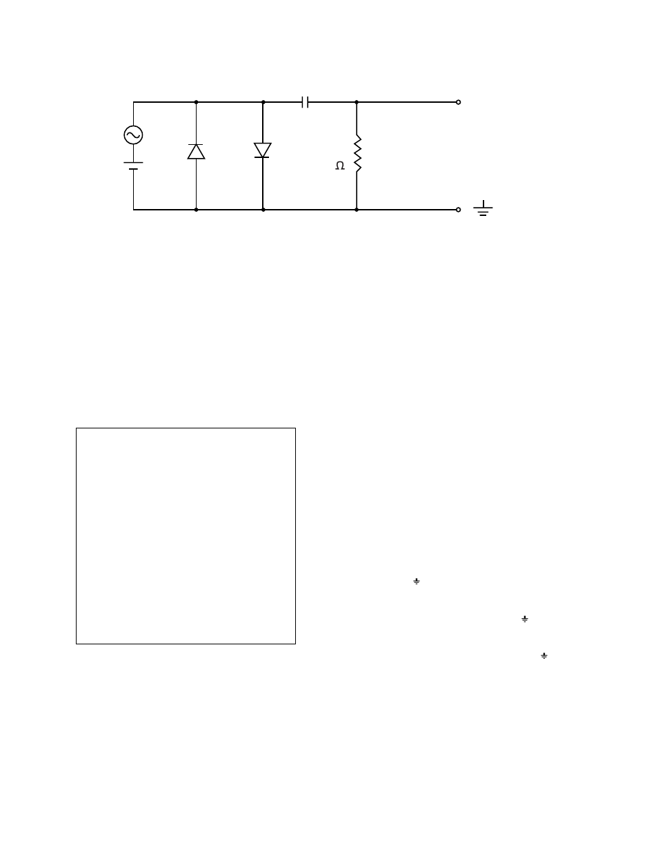
Figure 9-2. Recommended input conditioning circuit for period averaging.
An internal gain stage is used to amplify low-
level ac signals prior to a zero-crossing detector
for the period averaging measurement. The
minimum pulse width requirements increase
(maximum frequency decreases) with
increasing gain as shown in Table 9-7. Signals
larger than the specified maximum for a range
will saturate the gain stage and prevent
operation up to the maximum specified
frequency. A recommended input conditioning
circuit for period averaging measurements is
shown in Figure 9-2.
CAUTION: Noisy signals with slow
transitions through the zero voltage
threshold are problematic for period
measurements, because of the potential for
extraneous counts and the zero crossing
point. A zero-crossing detector with 10 mV
of hysteresis follows the voltage gain
stages. The effective input referred
hysteresis equals 10 mV divided by the
selected voltage gain. The effective input
referred hysteresis for range code X1 is
only 0.1 mV. Consequently, 0.1 mV of
noise on the input signal could cause
extraneous counts for range code X1. For
best results, select the smallest gain that
will meet the minimum input signal
requirements.
In Figure 9-2, the capacitor C is a dc blocking
capacitor for offset voltage removal. Resistor
R1 is used to bias the datalogger side of the
input circuit to ground. Low-level sensor
outputs can have dc offset voltages that prevent
the internal voltage comparator from ever
crossing its switch point. The reactance of the
dc blocking capacitor (Xc = (2
π f C)
-1
) and
resistor R1 form a voltage divider at low
frequencies (R1/(R1 + Xc)) that attenuates the
applied input signal. This attenuation sets a
lower limit on low-frequency operation and the
minimum size of R1. The circuit shown in
Figure 9-2 attenuates the input signal by a
factor of 2 at 16 Hz.
The back-to-back silicon diodes D1 and D2
shown in Figure 9-2 provide ESD protection for
capacitor C and the sensor, and also limit large
amplitude sensor signals. These diodes clip
large amplitude signals to approximately 1.4 V
pk-pk, which is within the recommended input
signal ranges for all range codes. Diodes D1
and D2 along with resistor R1 are
recommended to limit large amplitude sensor
signals, even when dc blocking capacitor C is
not used. Sensors outputting large voltages
may cause large currents to flow through these
back-to-back diodes. A current limiting resistor
may be desirable to minimize these currents in
some situations.
The current flow through these clipping diodes
may also induce single-ended offset voltages if
it returns into the
ground terminals because
of an alternate return path (ground loop) back to
the sensor. Single-ended offset voltages of up
to 1
µV/mA of current that flows into the
ground terminals can be induced across the
front panel. The back-to-back diodes can be
tied into the G ground terminals, rather than
ground terminals, if this is a problem.
PARAM.
DATA
NUM.
TYPE
DESCRIPTION
01:
2
Repetitions
02:
2
Output option/Range
code (Table 9-8)