I2c timing specifications, C timing specifications, Ds1875 – Rainbow Electronics DS1875 User Manual
Page 9: Pon triplexer and sfp controller
DS1875
Note 1:
All voltages are referenced to ground. Current into IC is positive, and current out of the IC is negative.
Note 2:
Digital inputs are at rail. FETG is disconnected. SDA = SCL = V
CC
. SW, DAC1, and M4DAC are not loaded.
Note 3:
See the
Safety Shutdown (FETG) Output section for details.
Note 4:
Eight ranges allow the full scale to change from 625mV to 2.5V.
Note 5:
Eight ranges allow the full scale to change from 312.5mV to 1.25V.
Note 6:
This specification applies to the expected full-scale value for the selected range. See the COMP RANGING register
description for available full-scale ranges.
Note 7:
The output impedance of the DS1875 is proportional to its scale setting. For instance, if using the 1/2 scale, the output
impedance would be approximately 1.56k
Ω.
Note 8:
This specification applies to the expected full-scale value for the selected range. See the MOD RANGING register
description for available full-scale ranges.
Note 9:
The switching frequency is selectable between four values: 131.25kHz, 262.5kHz, 525kHz, and 1050kHz.
Note 10: See the
APC and Quick-Trip Shared Comparator Timing section for details.
Note 11: Guaranteed by design.
Note 12: I
2
C interface timing shown is for fast-mode (400kHz) operation. This device is also backward compatible with I
2
C stan-
dard mode.
Note 13: C
B
—Total capacitance of one bus line in pF.
Note 14: EEPROM write begins after a STOP condition occurs.
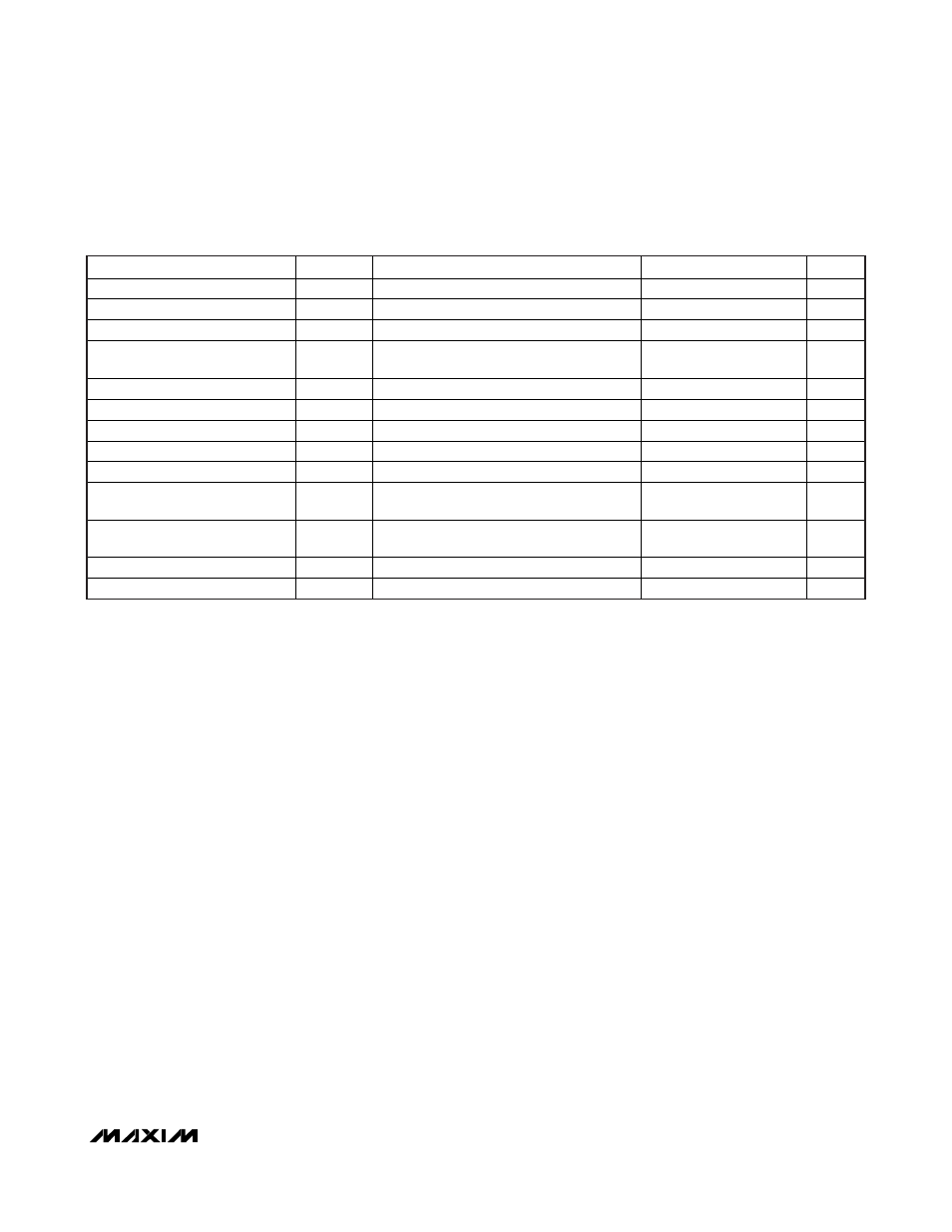
I
2
C TIMING SPECIFICATIONS
(V
CC
= +2.85V to +3.9V, T
A
= -40°C to +95°C, timing referenced to V
IL(MAX)
and V
IH(MIN)
.) (See Figure 15.)
PARAMETER
SYMBOL
CONDITIONS
MIN
TYP
MAX
UNITS
SCL Clock Frequency
f
SCL
(Note
12)
0
400 kHz
Clock Pulse-Width Low
t
LOW
1.3
μs
Clock Pulse-Width High
t
HIGH
0.6
μs
Bus-Free Time Between STOP
and START Condition
t
BUF
1.3
μs
START Hold Time
t
HD:STA
0.6
μs
START Setup Time
t
SU:STA
0.6
μs
Data in Hold Time
t
HD:DAT
0
0.9
μs
Data in Setup Time
t
SU:DAT
100
ns
Capacitive Load for Each Bus Line
C
B
400 pF
Rise Time of Both SDA and SCL
Signals
t
R
(Note
13)
20 +
0.1C
B
300 ns
Fall Time of Both SDA and SCL
Signals
t
F
(Note
13)
20 +
0.1C
B
300 ns
STOP Setup Time
t
SU:STO
0.6
μs
EEPROM Write Time
t
W
(Note
14)
20 ms
PON Triplexer and SFP Controller
_______________________________________________________________________________________
9