Pwm controller, Figure 11. pwm controller diagram, Table 7. mon3 hysteresis threshold values – Rainbow Electronics DS1875 User Manual
Page 25: Ds1875, Pon triplexer and sfp controller

DS1875
two thresholds. The actual threshold values are a func-
tion of the number of right-shifts being used. Table 7
shows the threshold values for each possible number
of right-shifts.
The RSSI_FF and RSSI_FC (Table 02h, Register 89h)
bits are used to force fine-mode or coarse-mode con-
versions, or to disable the dual-range functionality.
Dual-range functionality is enabled by default (both
RSSI_FC and RSSI_FF are factory programmed to 0 in
EEPROM). It can be disabled by setting RSSI_FC to 0
and RSSI_FF to 1. These bits are also useful when cali-
brating MON3. For additional information, see the
Memory Map
section.
PWM Controller
The DS1875 has a PWM controller that, when used with
external components, generates a low-noise, high-volt-
age output to bias APDs in optical receivers. The
achievable boost voltage is determined by the external
component selection. Figure 12 shows a typical
schematic. Selection of switching frequency, external
inductor, capacitors, resistor network, switching FET,
and switch diode determine the performance of the
DC-DC converter. The PWM controller can be config-
ured in boost or buck mode. Both modes require an
external nMOS or npn transistor.
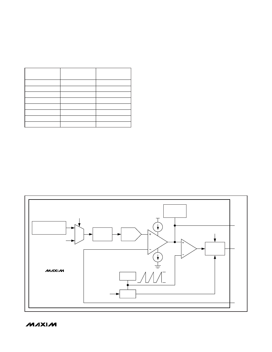
The DS1875 PWM controller consists of several sec-
tions used to create a PWM signal to drive a DC-DC
converter. Figure 11 is a block diagram of the DS1875
PWM controller. Following is a description of each
block in the PWM controller and some guidelines for
selecting components for the DC-DC converter.
The PWM DAC is used to set the desired output voltage
of the DC-DC converter section. The feedback from the
DC-DC converter is compared to the output from the
PWM DAC by an error amplifier. If the FB level is less
Table 7. MON3 Hysteresis Threshold Values
*
This is the minimum reported coarse-mode conversion.
NO. OF RIGHT-
SHIFTS
FINE MODE
(MAX)
COARSE MODE
(MIN*)
0 FFF8h
F000h
1 7FFCh
7800h
2 3FFEh
3C00h
3 1FFFh
1E00h
4 0FFFh
0F00h
5 07FFh
0780h
6 03FFh
03C0h
7 01FFh
01E0h
MUX
PWM DAC
8-BIT
0 TO 1.25V
10
μA
MANUAL I
2
C CONTROL
PWM_FR[1:0]
RAMP
90% DUTY
CYCLE OSC
SW
COMP
M3QT
1.9V
1.0V
FB
PWM EN
PWM CONTROLLER
GATE DRIVER
90% MAX
DUTY CYCLE
PWM DAC
TABLE 02h
REGISTER FEh
PWM DAC TEMPERATURE-
REFERENCED LUT
TABLE 07h
VOLTAGE CLAMP
HIGH = 2.1V
LOW = 0.8V
ERROR
AMPLIFIER
10
μA
DS1875
Figure 11. PWM Controller Diagram
PON Triplexer and SFP Controller
______________________________________________________________________________________
25
