Adc timing, Figure 4. m3qt timing, Figure 5. adc timing with en5to8b = 0 – Rainbow Electronics DS1875 User Manual
Page 20: Figure 6. adc timing with en5to8b = 1, Table 3. adc default monitor ranges, Ds1875 pon triplexer and sfp controller

DS1875
PON Triplexer and SFP Controller
20
______________________________________________________________________________________
The ADC results (after right-shifting, if used) are com-
pared to high and low alarm and warning thresholds
after each conversion. The alarm values can be used to
trigger the TX-F or FETG outputs. These ADC thresholds
are user programmable through the I
2
C interface, as
well as masking registers that can be used to prevent
the alarms from triggering the TX-F and FETG outputs.
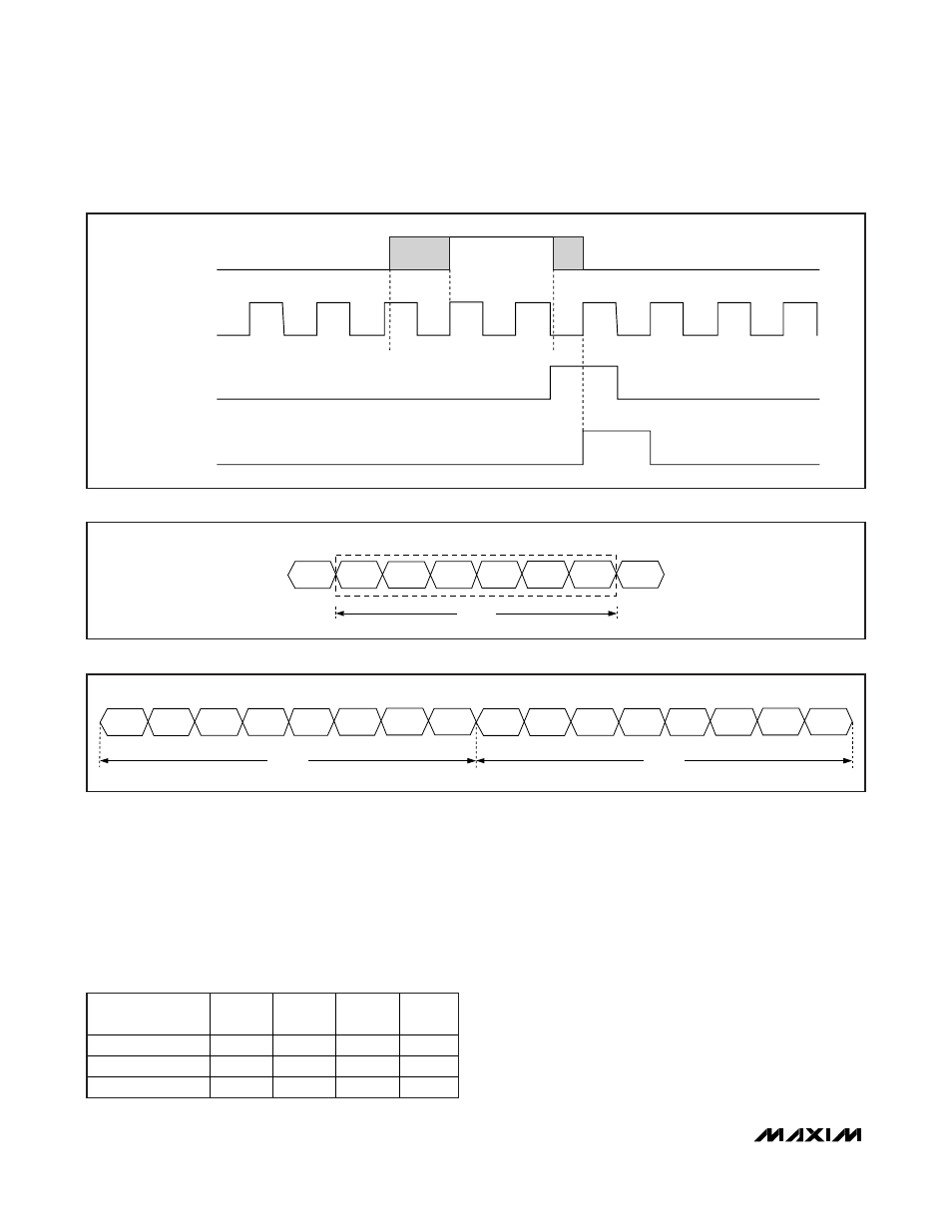
ADC Timing
There are 10 analog channels that are digitized in a
sequential fashion. The MON5–MON8 channels are
sampled depending on the state of the EN5TO8B bit in
Table 02h, Register 89h. If the bit is programmed to
logic 0, the ADC cycles through temperature, V
CC
, and
MON1–MON4 (Figure 5). If the bit is programmed to
logic 1, all 10 channels are digitized, including chan-
nels MON5–MON8 (Figure 6). In this mode (EN5TO8B
= 0), each of MON5–MON8 is sampled on alternate
cycles, as shown in Figure 5. The total time required to
convert one set of channels is the sequential ADC
cycle time, t
FRAME1
or t
FRAME2
(see Figure 6).
Table 3. ADC Default Monitor Ranges
SIGNAL
+FS
SIGNAL
+FS
HEX
-FS
SIGNAL
-FS
HEX
Temperature (°C)
127.996
7FFF
-128
8000
V
CC
(V)
6.5528
FFF8
0
0000
MON1–MON8 (V)
2.4997
FFF8
0
0000
V
CC
MON1
MON2
MON3
MON4
MON5
MON6
TEMP
V
CC
MON1
MON2
MON3
MON4
MON7
MON8
TEMP
t
FRAME2
t
FRAME2
Figure 6. ADC Timing with EN5TO8B = 1
TEMP
V
CC
MON1
MON2
MON3
MON4
TEMP
ONE ADC CYCLE
MON4
t
FRAME1
Figure 5. ADC Timing with EN5TO8B = 0
TRIP CONDITION
mCLK
(525kHz)
CAPTURE ALARM
M3QT ALARM
(UNLATCHED)
Figure 4. M3QT Timing
