Safety shutdown (fetg) output, Determining alarm causes usi, Determining alarm causes using the i – Rainbow Electronics DS1875 User Manual
Page 22: C interface, Ds1875 pon triplexer and sfp controller

DS1875
PON Triplexer and SFP Controller
22
______________________________________________________________________________________
Safety Shutdown (FETG) Output
The FETG output has masking registers (separate from
TX-F) for the ADC alarms and the QT alarms to select
which comparisons cause it to assert. Unlike TX-F, the
FETG output is always latched. Its output polarity is
programmable to allow an external nMOS or pMOS to
open during alarms to shut off the laser-diode current.
If the FETG output triggers, indicating that the DS1875
is in shutdown, it requires TX-D, SOFT TX-D, or cycling
power to be reset. Under all conditions, when the ana-
log outputs are reinitialized after being disabled, all the
alarms with the exception of the V
CC
low ADC alarm
are cleared. The V
CC
low alarm must remain active to
prevent the output from attempting to operate when
inadequate V
CC
exists to operate the laser driver. Once
adequate V
CC
is present to clear the V
CC
low alarm,
the outputs are enabled following the same sequence
as the power-up sequence.
As previously mentioned, the FETG is an output used to
disable the laser current through a series nMOS or
pMOS. This requires that the FETG output can sink or
source current. Because the DS1875 does not know if it
should sink or source current before V
CC
exceeds
V
POA
, which triggers the EE recall, this output is high
impedance when V
CC
is below V
POA
(see the
Low-
Voltage Operation
section for details and diagram). The
application circuit should use a pullup or pulldown
resistor on this pin that pulls FETG to the alarm/shut-
down state (high for a pMOS, low for a nMOS). Once
V
CC
is above V
POA
, the DS1875 pulls the FETG output
to the state determined by the FETG DIR bit (Table 02h,
Register 89h). Set FETG DIR to 0 if an nMOS is used
and 1 if a pMOS is used.
Determining Alarm Causes Using the I
2
C
Interface
To determine the cause of the TX-F or FETG alarm, the
system processor can read the DS1875’s alarm trap bytes
(ATB) through the I
2
C interface (Table 01h, Registers
F8h–FBh). The ATB has a bit for each alarm. Any time an
alarm occurs, regardless of the mask bit’s state, the
DS1875 sets the corresponding bit in the ATB. Active ATB
bits remain set until written to 0s through the I
2
C interface.
On power-up, the ATB is 0s until alarms dictate otherwise.
FETG causes additional alarms that make it difficult to
determine the root cause of the problem. Therefore, no
updates are made to the ATB when FETG occurs.
I
BIAS
V
MOD
DETECTION OF
FETG FAULT
t
OFF
t
ON
t
ON
t
OFF
TX-D
t
FETG:ON
FETG*
*FETG DIR = 0
t
FETG:OFF
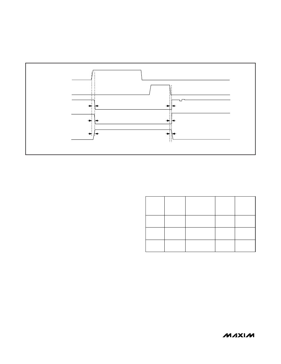
Figure 8. FETG/Output Disable Timing (Fault Condition Detected)
Table 5. FETG, MOD, and BIAS Outputs
as a Function of TX-D and Alarm Sources
V
CC
>
V
POA
TX-D
NONMASKED
FETG ALARM
FETG
MOD AND
BIAS
OUTPUTS
Yes 0
0
FETG
DIR
Enabled
Yes 0
1
FETG
DIR
Disabled
Yes 1
X
FETG
DIR
Disabled
