Die identification, Low-voltage operation, Enhanced rssi monitoring (du – Rainbow Electronics DS1875 User Manual
Page 23: Figure 9. see timing, Ds1875, Pon triplexer and sfp controller

DS1875
Die Identification
The DS1875 has an ID hard-coded to its die. Two regis-
ters (Table 02h, Registers 86h–87h) are assigned for
this feature. Byte 86h reads 75h to identify the part as
the DS1875; byte 87h reads the die revision.
Low-Voltage Operation
The DS1875 contains two power-on reset (POR) levels.
The lower level is a digital POR (V
POD
) and the higher
level is an analog POR (V
POA
). At startup, before the
supply voltage rises above V
POA
, the outputs are dis-
abled (FETG and BIAS outputs are high impedance,
MOD is low), all SRAM locations are low (including
shadowed EEPROM (SEE)), and all analog circuitry is
disabled. When V
CC
reaches V
POA
, the SEE is
recalled, and the analog circuitry is enabled. While V
CC
remains above V
POA
, the device is in its normal operat-
ing state, and it responds based on its nonvolatile con-
figuration. If during operation V
CC
falls below V
POA
but
is still above V
POD
, the SRAM retains the SEE settings
from the first SEE recall, but the device analog is shut
down and the outputs are disabled. FETG is driven to
its alarm state defined by the FETG DIR bit (Table 02h,
Register 89h). If the supply voltage recovers back
above V
POA
, the device immediately resumes normal
functioning. When the supply voltage falls below V
POD
,
the device SRAM is placed in its default state and
another SEE recall is required to reload the nonvolatile
settings. The EEPROM recall occurs the next time V
CC
exceeds V
POA
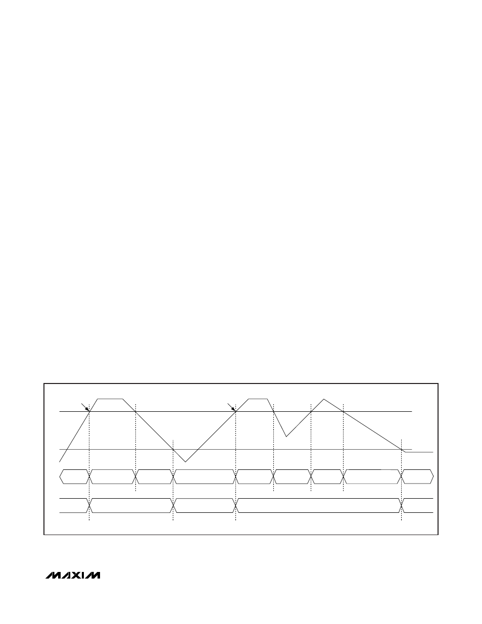
. Figure 9 shows the sequence of events
as the voltage varies.
Any time V
CC
is above V
POD
, the I
2
C interface can be
used to determine if V
CC
is below the V
POA
level. This
is accomplished by checking the RDYB bit in the status
(Lower Memory, Register 6Eh) byte. RDYB is set when
V
CC
is below V
POA
. When V
CC
rises above V
POA
,
RDYB is timed (within 500µs) to go to 0, at which point
the part is fully functional.
For all device addresses sourced from EEPROM (Table
02h, Register 8Ch), the default device address is A2h
until V
CC
exceeds V
POA
, allowing the device address
to be recalled from the EEPROM.
Enhanced RSSI Monitoring (Dual Range
Functionality)
The DS1875 offers a new feature to improve the accu-
racy and range of MON3, which is most commonly
used for monitoring RSSI. This feature enables right-
shifting (along with its gain and offset settings) when
the input signal is below a set threshold (within the
range that benefits using right-shifting) and then auto-
matically disables right-shifting (recalling different gain
and offset settings) when the input signal exceeds the
threshold. Also, to prevent “chattering,” hysteresis pre-
vents excessive switching between modes in addition
to ensuring that continuity is maintained. Dual range
operation is enabled by default (factory programmed in
EEPROM). However, it can easily be disabled through
the RSSI_FF and RSSI_FC bits. When dual range oper-
ation is disabled, MON3 operates identically to the
other MON channels, although featuring a differential
input.
V
CC
V
POA
V
POD
FETG
SEE
HIGH
IMPEDANCE
HIGH
IMPEDANCE
HIGH
IMPEDANCE
NORMAL
OPERATION
DRIVEN TO
FETG DIR
NORMAL
OPERATION
PRECHARGED
TO 0
PRECHARGED
TO 0
PRECHARGED
TO 0
RECALLED
VALUE
RECALLED
VALUE
DRIVEN TO
FETG DIR
NORMAL
OPERATION
DRIVEN TO
FETG DIR
SEE RECALL
SEE RECALL
Figure 9. SEE Timing
PON Triplexer and SFP Controller
______________________________________________________________________________________
23
