Bias and mod output as a fun, Apc and quick-trip shared co, Apc and quick-trip shared comparator timing – Rainbow Electronics DS1875 User Manual
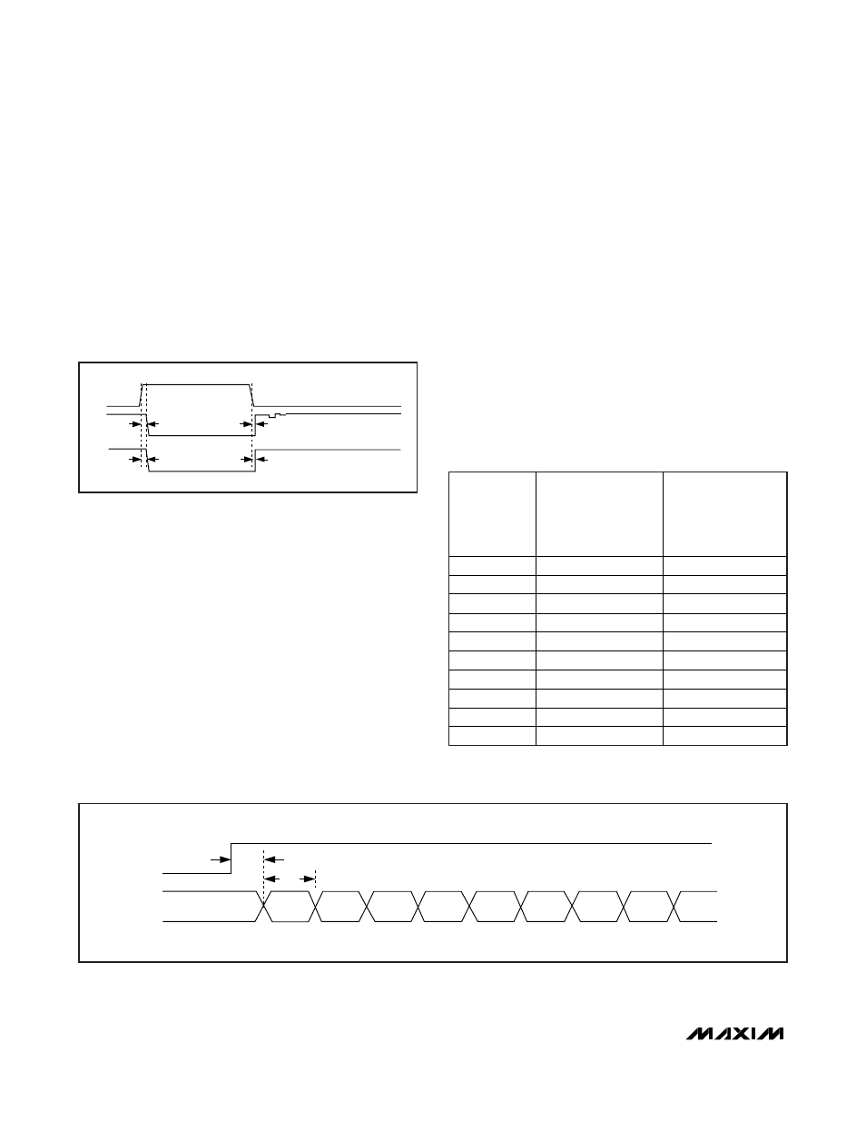
Page 18: Figure 2. tx-d timing, Figure 3. apc loop and quick-trip sample timing, Table 2. update rate timing, Ds1875 pon triplexer and sfp controller

DS1875
PON Triplexer and SFP Controller
18
______________________________________________________________________________________
BIAS and MOD Output as a Function of
Transmit Disable (TX-D)
If the TX-D pin is asserted (logic 1) during normal oper-
ation, the outputs are disabled within t
OFF
. When TX-D
is deasserted (logic 0), the DS1875 turns on the MOD
output with the value associated with the present tem-
perature and initializes the BIAS using the same search
algorithm used at startup. When asserted, the SOFT
TX-D bit (Lower Memory, Register 6Eh) offers a soft-
ware control identical to the TX-D pin (see Figure 2).
APC and Quick-Trip Shared Comparator
Timing
As shown in Figure 3, the DS1875’s input comparator is
shared between the APC control loop and the three
quick-trip alarms (TXP HI, TXP LO, and BIAS HI). The
comparator polls the alarms in a multiplexed sequence.
Six of every eight comparator readings are used for
APC loop-bias current control. The other two updates
are used to check the HTXP/LTXP (monitor diode volt-
age) and the HBIAS (MON1) signals against the inter-
nal APC and BIAS reference. If the last APC
comparison was higher than the APC set point, it
makes an HTXP comparison, and if it is lower, it makes
an LTXP comparison. Depending on the results of the
comparison, the corresponding alarms and warnings
(TXP HI, TXP LO) are asserted or deasserted.
The DS1875 has a programmable comparator sample
time based on an internally generated clock to facilitate
a wide variety of external filtering options suitable for
burst-mode transmitters. The rising edge of BEN trig-
gers the sample to occur, and the Update Rate register
(Table 02h, Register 88h) determines the sampling time.
The first sample occurs (t
FIRST
) after the rising edge of
BEN. The internal clock is asynchronous to BEN, caus-
ing a ±50ns uncertainty regarding when the first sample
will occur following BEN. After the first sample occurs,
subsequent samples occur on a regular interval, t
REP
.
Table 2 shows the sample rate options available.
Updates to the TXP HI and TXP LO quick-trip alarms do
not occur during the BEN low time. The BIAS HI quick
trip can be sampled during the burst-low time. Any
*
All codes greater than 1001b (1010b to 1111b) use the
maximum sample time of code 1001b.
BEN
APC QUICK-TRIP
SAMPLE TIMES
HBIAS
SAMPLE
t
FIRST
t
REP
HTXP/LTXP
SAMPLE
APC
SAMPLE
APC
SAMPLE
APC
SAMPLE
APC
SAMPLE
APC
SAMPLE
APC
SAMPLE
APC
SAMPLE
Figure 3. APC Loop and Quick-Trip Sample Timing
Table 2. Update Rate Timing
APC_SR[3:0]
MINIMUM TIME
FROM BEN TO
FIRST SAMPLE
(tFIRST) ±50ns
(ns)
REPEATED
SAMPLE PERIOD
FOLLOWING FIRST
SAMPLE (tREP)
(ns)
0000b
350
800
0001b
550
1200
0010b
750
1600
0011b
950
2000
0100b
1350
2800
0101b
1550
3200
0110b
1750
3600
0111b
2150
4400
1000b
2950
6000
1001b*
3150
6400
TX-D
I
BIAS
V
MOD
t
OFF
t
ON
t
ON
t
OFF
Figure 2. TX-D Timing
