Pwm characteristics, Timing characteristics (cont, Ds1875 – Rainbow Electronics DS1875 User Manual
Page 7: Pon triplexer and sfp controller
DS1875
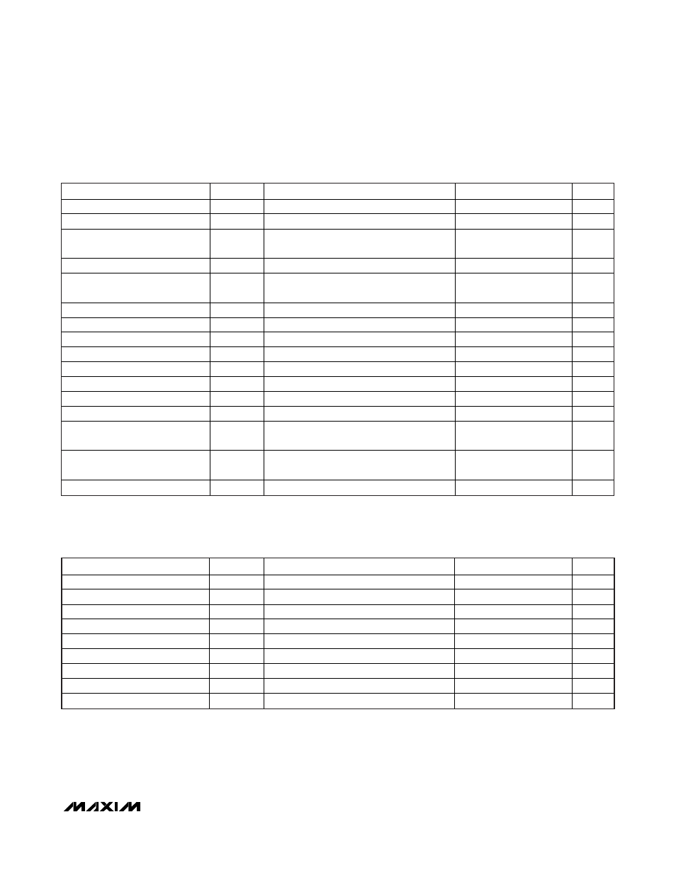
PARAMETER SYMBOL
CONDITIONS
MIN
TYP
MAX
UNITS
PWM-DAC Full-Scale Voltage
V
PWM-DAC
1.25
V
PWM-DAC Resolution
8
Bits
V
PWM-DAC
Full-Scale Voltage
Error
T
A
= +25°C
1.25
%
V
PWM-DAC
Integral Nonlinearity
-1
1
LSB
V
PWM-DAC
Differential
Nonlinearity
-1 1 LSB
V
PWM-DAC
Temperature Drift
-2
+2
%FS
SW Output Impedance
20
SW Frequency Error
f
SWER
(Note
9)
-5
+7
%
SW Duty Cycle
D
MAX
89 90 91 %
Error-Amplifier Source Current
-10
μA
Error-Amplifier Sink Current
+10
μA
COMP High-Voltage Clamp
2.1
V
COMP Low-Voltage Clamp
0.8
V
Error-Amplifier
Transconductance
G
M
425
μS
Error-Amplifier Output
Impedance
R
EA
260
M
FB Pin Capacitance
5
pF
PARAMETER
SYMBOL
CONDITIONS
MIN
TYP
MAX
UNITS
First BMD Sample Following BEN
t
FIRST
(Note
10)
Remaining Updates During BEN
t
UPDATE
(Note
10)
BEN High Time
t
BEN:HIGH
400
ns
BEN Low Time
t
BEN:LOW
96
ns
Output-Enable Time Following POA
t
INIT
10
ms
BIAS and MOD Turn-Off Delay
t
OFF
5
μs
BIAS and MOD Turn-On Delay
t
ON
5
μs
FETG Turn-On Delay
t
FETG:ON
5
μs
FETG Turn-Off Delay
t
FETG:OFF
5
μs
TIMING CHARACTERISTICS (CONTROL LOOP AND QUICK TRIP)
(V
CC
= +2.85V to +3.9V, T
A
= -40°C to +95°C, unless otherwise noted.)
PWM CHARACTERISTICS
(V
CC
= +2.85V to +3.9V, T
A
= -40°C to +95°C, unless otherwise noted.)
PON Triplexer and SFP Controller
_______________________________________________________________________________________
7