Rainbow Electronics DS2151Q User Manual
Page 4
DS2151Q
022697 4/46
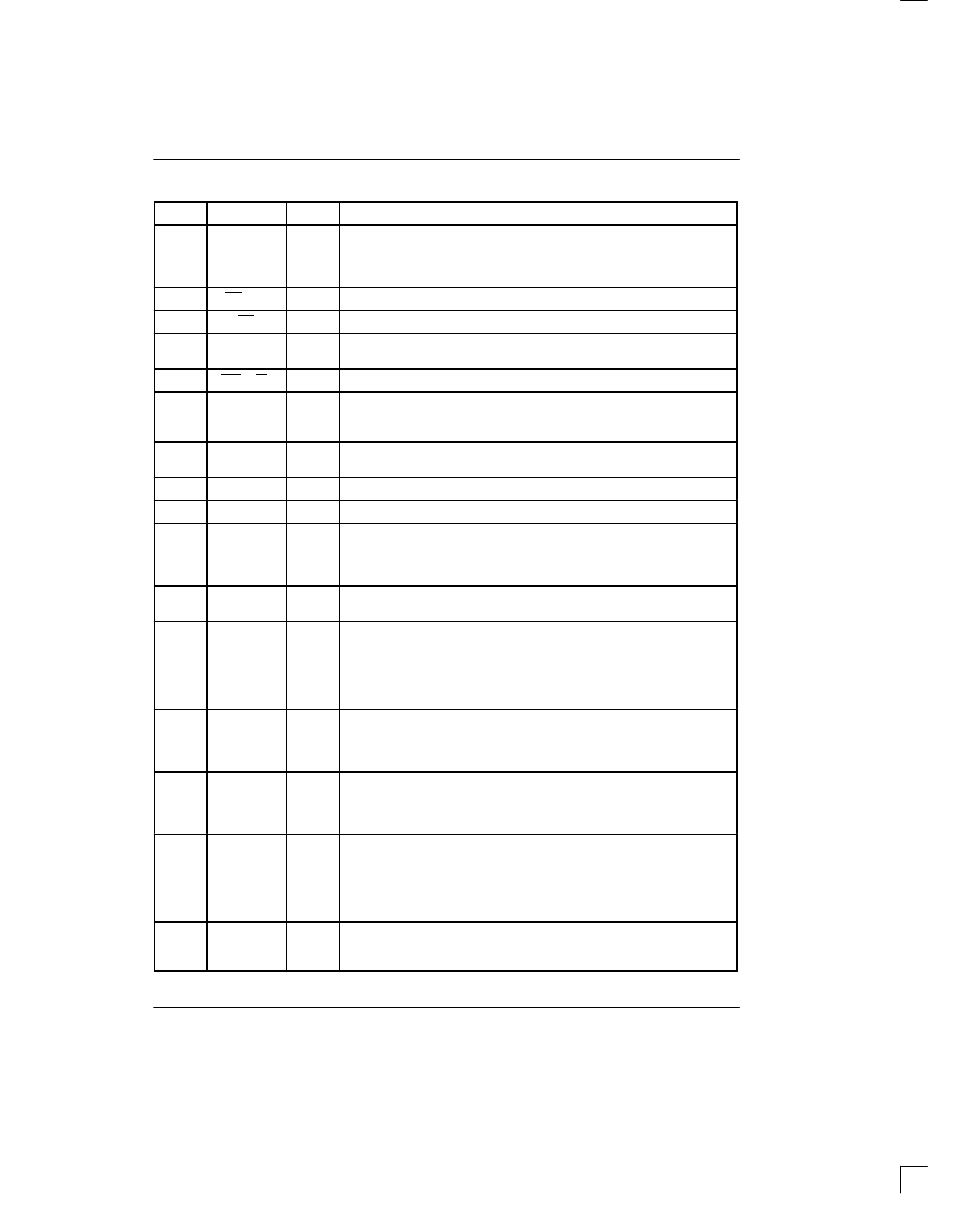
PIN DESCRIPTION Table 1–1
PIN
SYMBOL
TYPE
DESCRIPTION
1
2
3
4
AD4
AD5
AD6
AD7
I/O
Address/Data Bus. An 8–bit multiplexed address/data bus.
5
RD(DS)
I
Read Input (Data Strobe).
6
CS
I
Chip Select. Must be low to read or write the port.
7
ALE(AS)
I
Address Latch Enable (Address Strobe). A positive going edge serves to
demultiplex the bus.
8
WR(R/W)
I
Write Input (Read/Write).
9
RLINK
O
Receive Link Data. Updated with either FDL data (ESF) or Fs bits (D4) or
Z bits (ZBTSI) one RCLK before the start of a frame. See Section 13 for tim-
ing details.
10
RLCLK
O
Receive Link Clock. 4 KHz or 2 KHz (ZBTSI) demand clock for the RLINK
output. See Section 13 for timing details.
11
DVSS
–
Digital Signal Ground. 0.0 volts. Should be tied to local ground plane.
12
RCLK
O
Receive Clock. Recovered 1.544 MHz clock.
13
RCHCLK
O
Receive Channel Clock. 192 KHz clock which pulses high during the LSB
of each channel. Useful for parallel to serial conversion of channel data,
locating Robbed–Bit signaling bits, and for blocking clocks in DDS applica-
tions. See Section 13 for timing details.
14
RSER
O
Receive Serial Data. Received NRZ serial data, updated on rising edges
of RCLK or SYSCLK.
15
RSYNC
I/O
Receive Sync. An extracted pulse, one RCLK wide, is output at this pin which
identifies either frame (RCR2.4=0) or multiframe boundaries (RCR2.4=1). If
set to output frame boundaries, then via RCR2.5, RSYNC can also be set to
output double–wide pulses on signaling frames. If the elastic store is enabled
via the CCR1.2, then this pin can be enabled to be an input via RCR2.3 at
which a frame boundary pulse is applied. See Section 13 for timing details.
16
RLOS/LOTC
O
Receive Loss of Sync/Loss of Transmit Clock. A dual function output.
If CCR3.5=0, will toggle high when the synchronizer is searching for the T1
frame and multiframe; if CCR3.5=1, will toggle high if the TCLK pin has not
toggled for 5us.
17
SYSCLK
I
System Clock. 1.544 MHz or 2.048 MHz clock. Only used when the elastic
store functions are enabled via either CCR1.7 or CCR1.2. Should be tied low
in applications that do not use the elastic store. If tied high for more than
100us, will force all output pins (including the parallel port) to 3–state.
18
RCHBLK
O
Receive Channel Block. A user programmable output that can be forced
high or low during any of the 24 T1 channels. Useful for blocking clocks to
a serial UART or LAPD controller in applications where not all T1 channels
are used such as Fractional T1, 384K bps service, 768K bps, or ISDN–PRI.
Also useful for locating individual channels in drop–and–insert applications.
See Section 13 for timing details.
19
ACLKI
I
Alternate Clock Input. Upon a receive carrier loss, the clock applied at this
pin (normally 1.544 MHz) will be routed to the RCLK pin. If no clock is routed
to this pin, then it should be tied to DVSS.