Rainbow Electronics DS2151Q User Manual
Page 28
DS2151Q
022697 28/46
12.0 LINE INTERFACE FUNCTIONS
The line interface function in the DS2151Q contains
three sections; (1) the receiver which handles clock and
data recovery, (2) the transmitter which waveshapes
and drives the T1 line, and (3) the jitter attenuator. Each
of the these three sections is controlled by the Line Inter-
face Control Register (LICR) which is described below.
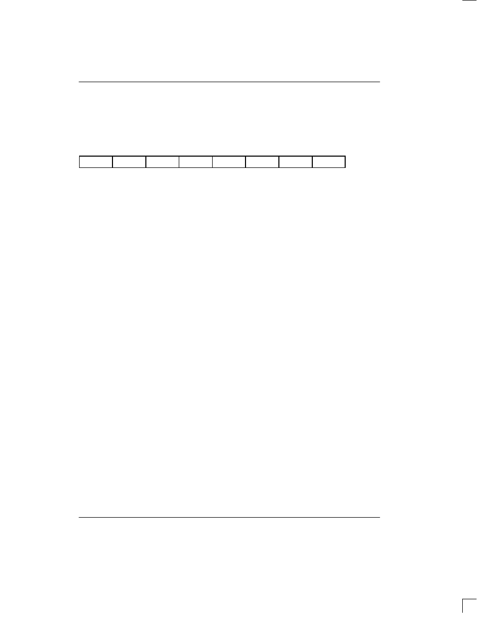
LICR: LINE INTERFACE CONTROL REGISTER (Address=7C Hex)
(MSB)
(LSB)
L2
L1
L0
EGL
JAS
JABDS
DJA
TPD
SYMBOL
POSITION
NAME AND DESCRIPTION
L2
LICR.7
Line Build Out Select Bit 2. Sets the transmitter build out; see the Table
12–2
L1
LICR.6
Line Build Out Select Bit 1. Sets the transmitter build out; see the Table 12–2
L0
LICR.5
Line Build Out Select Bit 0. Sets the transmitter build out; see the Table 12–2
EGL
LICR.4
Receive Equalizer Gain Limit.
0= –36 dB
1= –30 dB
JAS
LICR.3
Jitter Attenuator Select.
0=place the jitter attenuator on the receive side
1=place the jitter attenuator on the transmit side
JABDS
LICR.2
Jitter Attenuator Buffer Depth Select .
0=128 bits
1=32 bits (use for delay sensitive applications)
DJA
LICR.1
Disable Jitter Attenuator.
0=jitter attenuator enabled
1=jitter attenuator disabled
TPD
LICR.0
Transmit Power Down.
0=normal transmitter operation
1=powers down the transmitter and 3–states the TTIP and TRING pins
12.1 Receive Clock and Data Recovery
The DS2151Q contains a digital clock recovery system.
See the DS2151Q Block Diagram in Section 1 and Fig-
ure 12–1 for more details. The DS2151Q couples to the
receive T1 twisted pair via a 1:1 transformer. See Table
12–3 for transformer details. The DS2151Q automati-
cally adjusts to the T1 signal being received at the RTIP
and RRING pins and can handle T1 lines from 0 feet to
over 6000 feet in length. The crystal attached at the
XTAL1 and XTAL2 pins is multiplied by four via an inter-
nal PLL and fed to the clock recovery system. The clock
recovery system uses both edges of the clock from the
PLL circuit to form a 32 times oversampler which is used
to recover the clock and data. This oversampling tech-
nique offers outstanding jitter tolerance (see Figure
12–2). The EGL bit in the Line Interface Control Regis-
ter is used to limit the sensitivity of the receiver in the
DS2151Q. For most CPE applications, a receiver sen-
sitivity of –30 dB is wholly sufficient and hence the EGL
bit should be set to one. In some applications, more
sensitivity than –30 dB may be required and the
DS2151Q will allow the receiver to go as low as –36 dB if
the EGL bit is set to zero. However when the EGL bit is
set to zero, the DS2151Q will be more susceptible to
crosstalk and its jitter tolerance will suffer.
Normally, the clock that is output at the RCLK pin is the
recovered clock from the T1 AMI waveform presented
at the RTIP and RRING inputs. When no AMI signal is
present at RTIP and RRING, a Receive Carrier Loss
(RCL) condition will occur and the RCLK can be sourced
from either the ACLKI pin or from the crystal attached to
the XTAL1 and XTAL2 pins. The DS2151Q will sense
the ACLKI pin to determine if a clock is present. If no
LICR