1 i/o signal multiplexing (iomx), I/o signal multiplexing (iomx), Table 5-12 – Motorola CPCI-6115 User Manual
Page 107: Multiplexing sequence of the iomx function, Figure 5-5, Signal multiplexing diagram

Asynchronous Serial Ports
Transition Module Preparation and Installation
CPCI-6115 CompactPCI Single Board Computer Installation and Use (6806800A68D)
105
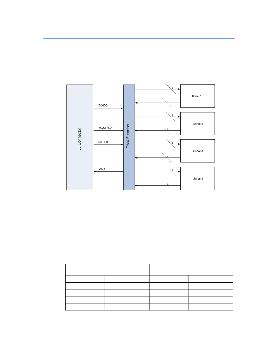
Due to pin limitations of the J5 connector, the CPCI-6115 SBC multiplexes the serial channel
control signals between the CPCI-6115 SBC and the CPCI-6115-MCPTM. This hardware
function is transparent to software. The block diagram for the signal multiplexing on the
transition module is shown in the following figure:
5.7.6.1
I/O Signal Multiplexing (IOMX)
The CPCI-6115-MCPTM uses a PLD to generate the IOMUX function. The CPCI-6115 SBC
uses a similar device. There are four pins that are used for the IOMX function: MXCLK,
MXSYNC#, MXDO and MXDI. MXCLK is the 10 MHz bit clock for the time-multiplexed data
lines MXDO and MXDI. MXSYNC# is asserted for one bit time at Time Slot 15 by the CPCI-
6115 SBC. MXSYNC# is used by the CPCI-6115-MCPTM to synchronize with the CPCI-6115
SBC. MXDO is the time-multiplexed output line from the CPCI-6115 and MXDI is the time-
multiplexed line from the CPCI-6115-MCPTM. A 16-to-1 multiplexing scheme is used with a 10
MHz bit rate. Sixteen time slots are defined and allocated as follows:
Figure 5-5
Signal Multiplexing Diagram
Table 5-12 Multiplexing Sequence of the IOMX Function
MXDO
(From CPCI-6115 SBC)
MXDI
(From CPCI-6115-MCPTM or CPCI-6106)
Time Slot
Signal Name
Time Slot
Signal Name
0
RTS3
0
CTS3
1
DTR3
1
DSR3
2
RTS1
2
DCD3
3
RTS2
3
CTS1
