3 sim bus clock control and generation, 1 bus timing, Sim bus clock control and generation – Freescale Semiconductor MC68HC08KH12 User Manual
Page 65: Bus timing, Sim clock signals, Signal name conventions
MC68HC(7)08KH12
—
Rev. 1.1
Advance Information
Freescale Semiconductor
65
shows the internal signal names used in this section.
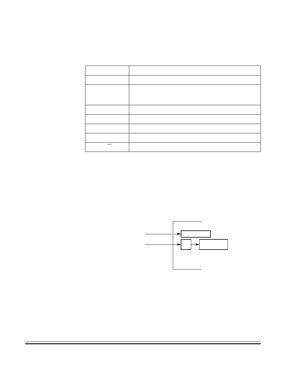
7.3 SIM Bus Clock Control and Generation
The bus clock generator provides system clock signals for the CPU and
peripherals on the MCU. The system clocks are generated from an
incoming clock, CGMOUT, as shown in
.
Figure 7-3. SIM Clock Signals
7.3.1 Bus Timing
In user mode, the internal bus frequency is the oscillator frequency
(CGMXCLK) divided by four.
Table 7-1. Signal Name Conventions
Signal Name
Description
CGMXCLK
Buffered OSC1 from the oscillator
CGMOUT
The CGMXCLK frequency divided by two. This signal is again
divided by two in the SIM to generate the internal bus clocks
(Bus clock = CGMXCLK divided by four)
IAB
Internal address bus
IDB
Internal data bus
PORRST
Signal from the power-on reset module to the SIM
IRST
Internal reset signal
R/W
Read/write signal
÷
2
BUS CLOCK
GENERATORS
SIM
SIM COUNTER
From
PLL/OSCILLATOR
From
PLL/OSCILLATOR
CGMOUT
CGMXCLK