Cgm i/o register summary, Table 8-2, Is a summary of – Freescale Semiconductor MC68HC08KH12 User Manual
Page 101
MC68HC(7)08KH12
—
Rev. 1.1
Advance Information
Freescale Semiconductor
101
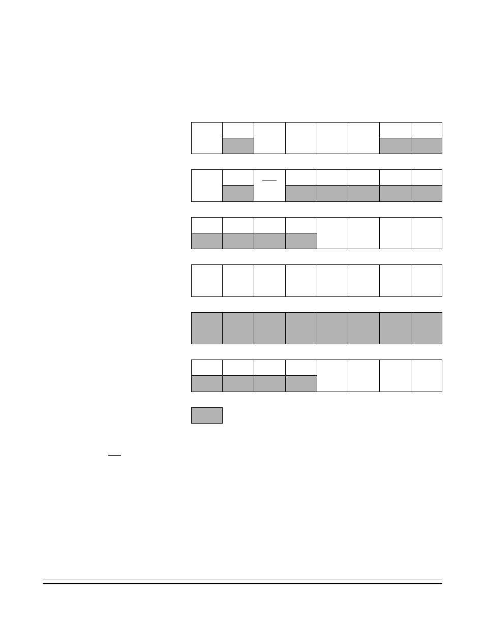
Table 8-2. CGM I/O Register Summary
Addr.
Register Name
Bit 7
6
5
4
3
2
1
Bit 0
$003A
PLL Control Register
(PCTL)
Read:
PLLIE
PLLF
PLLON
BCS
PRE1
PRE2
0
0
Write:
Reset:
0
0
1
0
1
0
0
0
$003B
PLL Bandwidth Control
Register
(PBWC)
Read:
AUTO
LOCK
ACQ
0
0
0
0
0
Write:
Reset:
0
0
0
0
0
0
0
0
$003C
PLL Multiplier Select
Register High
(PMSH)
Read:
0
0
0
0
MUL11
MUL10
MUL9
MUL8
Write:
Reset:
0
0
0
0
0
0
0
0
$003D
PLL Multiplier Select
Register Low
(PMSL)
Read:
MUL7
MUL6
MUL5
MUL4
MUL3
MUL2
MUL1
MUL0
Write:
Reset:
0
0
0
0
0
0
1
0
$003E
Unimplemented
Read:
Write:
Reset:
$003F
PLL Reference Divider
Select Register
(PRDS)
Read:
0
0
0
0
RDS3
RDS2
RDS1
RDS0
Write:
Reset:
0
0
0
0
0
0
0
1
= Unimplemented
NOTES:
1. When AUTO = 0, PLLIE is forced clear and is read-only.
2. When AUTO = 0, PLLF and LOCK read as clear.
3. When AUTO = 1, ACQ is read-only.
4. When PLLON = 0 or VRS7:VRS0 = $0, BCS is forced clear and is read-only.
5. When PLLON = 1, the PLL programming register is read-only.
6. When BCS = 1, PLLON is forced set and is read-only.