7 control timing, 8 oscillator characteristics, Control timing – Freescale Semiconductor MC68HC08KH12 User Manual
Page 251: Oscillator characteristics, 7 control timing 17.8 oscillator characteristics
MC68HC(7)08KH12
—
Rev. 1.1
Advance Information
Freescale Semiconductor
251
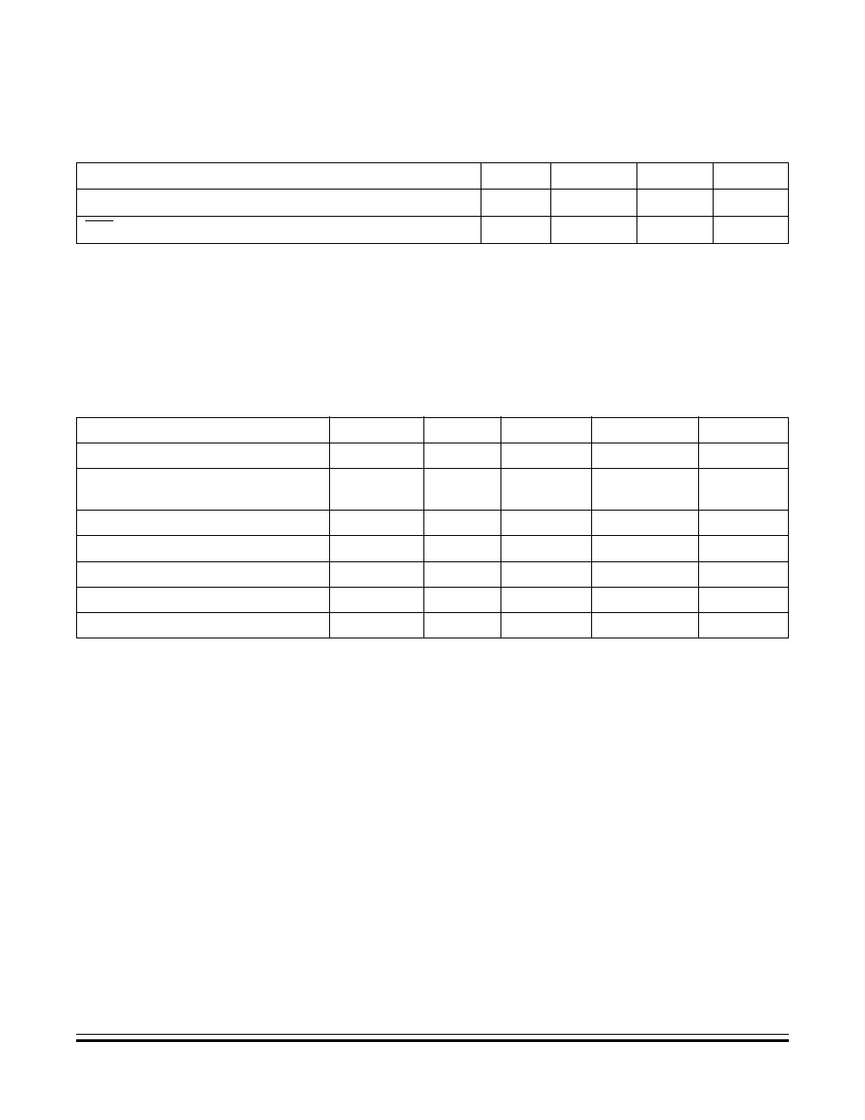
17.7 Control Timing
17.8 Oscillator Characteristics
Characteristic
Symbol
Min
Max
Unit
Internal Operating Frequency
(2)
f
OP
—
6
MHz
RST Input Pulse Width Low
(3)
t
IRL
50
—
ns
NOTES:
1. V
DD
= 4.0 to 5.5 Vdc, V
SS
= 0 Vdc; timing shown with respect to 20% V
DD
and 70% V
DD
, unless otherwise noted.
2. Some modules may require a minimum frequency greater than dc for proper operation; see appropriate table for this
information.
3. Minimum pulse width reset is guaranteed to be recognized. It is possible for a smaller pulse width to cause a reset.
Characteristic
Symbol
Min
Typ
Max
Unit
Crystal Frequency
(1)
f
CGMXCLK
—
6
—
MHz
External Clock
Reference Frequency
(1), (2)
f
CGMXCLK
dc
—
24
MHz
Crystal Load Capacitance
(3)
C
L
—
—
—
Crystal Fixed Capacitance
(3)
C
1
—
2
×
C
L
—
Crystal Tuning Capacitance
(3)
C
2
—
2
×
C
L
—
Feedback Bias Resistor
R
B
—
10
—
M
Ω
Series Resistor
(3), (4)
R
S
—
—
—
NOTES:
1. The USB module is designed to function at f
CGMXCLK
= 6MHz and CGMVCLK = 48MHz. The values given here are
oscillator specifications.
2. No more than 10% duty cycle deviation from 50%
3. Consult crystal vendor data sheet
4. Not Required for high frequency crystals