Power supply pins, Power supply bypassing – Freescale Semiconductor MC68HC08KH12 User Manual
Page 29
MC68HC(7)08KH12
—
Rev. 1.1
Advance Information
Freescale Semiconductor
29
1.5.2 Power Supply Pins (V
DDA
, V
SSA
, V
DD1
, V
SS1
, V
DD2
, and V
SS2
)
V
DDA
and V
SSA
are the analog power supply and ground pins used by
the on-chip Phase-Locked Loop circuit.
V
DD2
and V
SS2
are the power supply and ground pins used by the
internal circuitry of the chip.
V
DD1
and V
SS1
are the power supply and ground pins to the I/O pads.
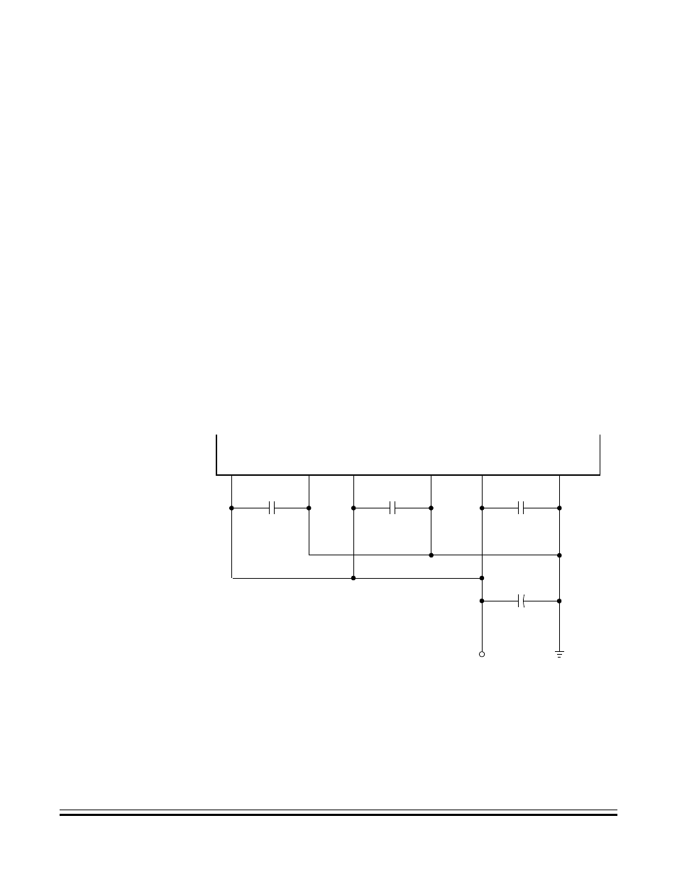
The MCU operates from a single power supply.
Fast signal transitions on MCU pins place high, short-duration current
demands on the power supply. To prevent noise problems, take special
care to provide power supply bypassing at the MCU as
shows. Place the bypass capacitors as close to the MCU power pins as
possible. Use high-frequency-response ceramic capacitors for C
BYPASS
.
C
BULK
are optional bulk current bypass capacitors for use in applications
that require the port pins to source high current levels.
Figure 1-3. Power Supply Bypassing
MCU
C
BULK
C
BYPASS
10nF
V
SS1
+
NOTE: Values shown are typical values.
V
DD2
C
BYPASS
10nF
V
DD2
C
BYPASS
10nF
V
SS2
V
SSA
V
DDA
Vbus