FUJITSU MB86617A User Manual
Page 9
LSI S pecification
MB86617A
Rev.1.0
Fujitsu VLSI
4
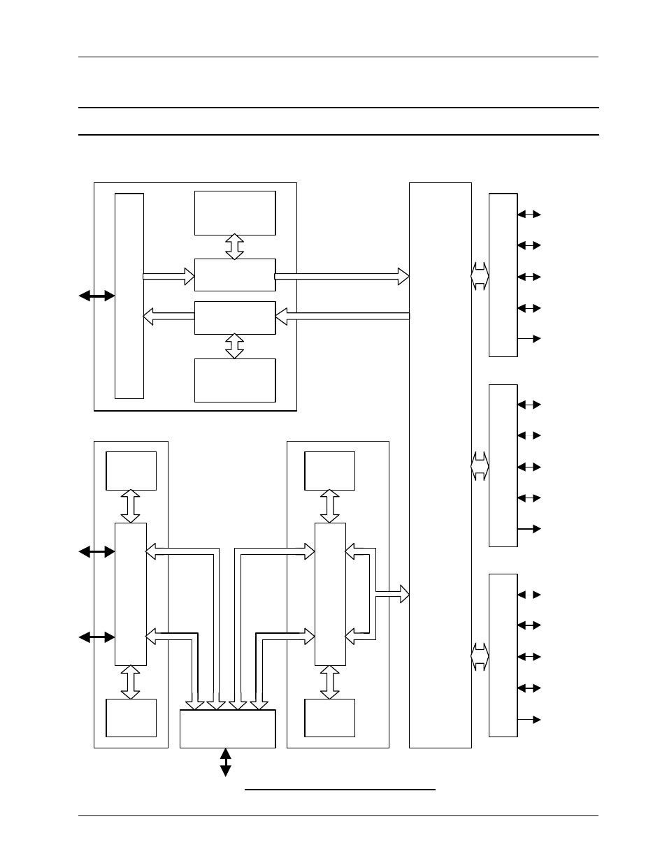
3.1. Block Diagram
MB86617A block diagram is shown below.
<
< Normal Operation Mode
Fig.3.1.1 Block Diagram - Normal Operation Mode -
1394 Interface (Port 0)
TPA0
XTPA0
TPB0
XTPB0
TPBIAS0
1394 Interface (Port 1)
TPA1
XTPA1
TPB1
XTPB1
TPBIAS1
1394 Interface (Port 2)
TPA2
XTPA2
TPB2
XTPB2
TPBIAS2
PHY/
LINK
Layer
Control
Circuit
CP IC
Interface
FIFO
(2KByte)
FIFO
(2KByte
)
Asynch Transmit
Exclusive FIFO
(256 byte)
Asynch Transmit
Exclusive FIFO
(256 byte)
TSP IC Interface
FIFO
(2KByte)
FIFO
(2KByte)
Asynch Transmit
Packet Process
Host Interface
Asynch Transmit
Packet Process
Data Bridge
See also other documents in the category FUJITSU Hardware:
- XG Series P3NK-4452-01ENZD (614 pages)
- FPCAC14C (1 page)
- MCJ3230SS (161 pages)
- MBA3073NC (138 pages)
- T5140 (102 pages)
- T5140 (76 pages)
- MAM3367MC/MP (152 pages)
- MPC3045AH (185 pages)
- MB2142-02 (23 pages)
- MB15F86UL (6 pages)
- MHS2030AT (40 pages)
- MHW2100BS (296 pages)
- MHK2060AT (227 pages)
- Disk Drives MHK2060AT (227 pages)
- MCM3064SS (170 pages)
- Mainboard D1561 (45 pages)
- MHC2040AT (219 pages)
- D1961 (45 pages)
- DISK DRIVES MHM2100AT (231 pages)
- MHR2010AT (250 pages)
- MHZ2120BJ (320 pages)
- MCE3064AP (175 pages)
- LQFP-64P (16 pages)
- Solaris PCI GigabitEthernet 3.0 (115 pages)
- MAY2036RC (94 pages)
- MAB3091 (142 pages)
- MPE3XXXAT (191 pages)
- MHV2040AH (40 pages)
- MHW2040AC (278 pages)
- ETERNUSmgr P2X0-0202-01EN (64 pages)
- VSS Hardware Provider 2.1 (134 pages)
- MAG3182FC (61 pages)
- MAU3147NC/NP (130 pages)
- MAX3147RC (94 pages)
- MHV2160BT (296 pages)
- MHV2040AT (280 pages)
- MAW3300NC/NP (130 pages)
- DeskPower E623 (50 pages)
- MAG3182LC (133 pages)
- OPTICAL DISK DRIVES MDG3064UB (42 pages)
- MHF2021AT (225 pages)
- MHR2040AT (40 pages)
- Single Drive FTM7926FB (1 page)
- PG-FCS103 (98 pages)
- MAS3735FC (114 pages)