Isochronous interface – FUJITSU MB86617A User Manual
Page 19
LSI S pecification
MB86617A
Rev.1.0
Fujitsu VLSI
14
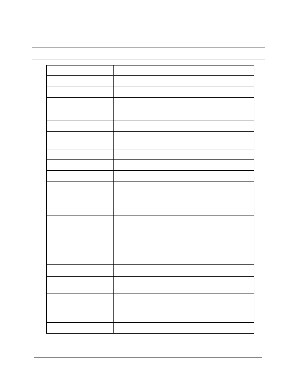
5.2. Isochronous Interface
This section explains the pin function of Isochronous interface.
Signal Name
I/O
Function
TSVALIDA
I/O
I.O pin for indicating effective data period of TS packet (on port A)
‘H’ active signal
TSSYNCA
I/O
Input/Output pin for indicating leading data of TS packet (on port A)
‘H’ active signal
TSCLKA
I/O
On transmitting: sync clock input pin for input data of TS packet
On receiving
: sync clock output pin for output data of TS packet
(switchable either 6.144MHz or 3.072MHz)
TSDA7 - 0
I/O
I/O pin for TS packet data (on Port A)
TSCGMSA
I
Serial input pin for CGMS and TSCH information (on port A)
Effective for 8 clocks since TSSYNCA input signal rising
SELIOA
O
Output pin for switching I/O on port A
Outputs ‘L’ at transmitting and ‘H’at receiving
SELTSPA
O
Output pin for switching output device from port A
TSVALIDB
I/O
I.O pin for indicating effective data period of TS packet (on port B)
‘H’ active signal
TSSYNCB
I/O
Input/Output pin for indicating leading data of TS packet (on port B)
‘H’ active signal
TSCLKB
I/O
On transmitting: sync clock input pin for input data of TS packet
On receiving
: sync clock output pin for output data of TS packet
(switchable either 6.144MHz or 3.072MHz)
TSDB7 - 0
I/O
I/O pin for TS packet data (on port B)
TSCGMSB
I
Serial input pin for CGMS and TSCH information (on port B)
Effective for 8 clocks since TSSYNCA input signal rising
SELIOB
O
Output pin for switching I/O on port B
Outputs ‘L’ at transmitting and ‘H’at receiving
SELTSPB
O
Output pin for switching output device from port B
ICLK
I
Clock input pin from DV-IC
XILWRE
O
Output pin for signal to be allowed accessing to Isochronous-FIFO
Asserted by completing reception of data for one source packet
‘L’ active signal
XIV
I
Input signal for enable signal of Isochronous data
Output Isochronous- FIFO data to data output pin while this signal in active.
Switch data synchronizing with rise edge of ICLK
XFP
O
Output pin of time stamp trigger signal
‘L’ active signal