Ieee1394 interface – FUJITSU MB86617A User Manual
Page 18
LSI S pecification
MB86617A
Rev.1.0
Fujitsu VLSI
13
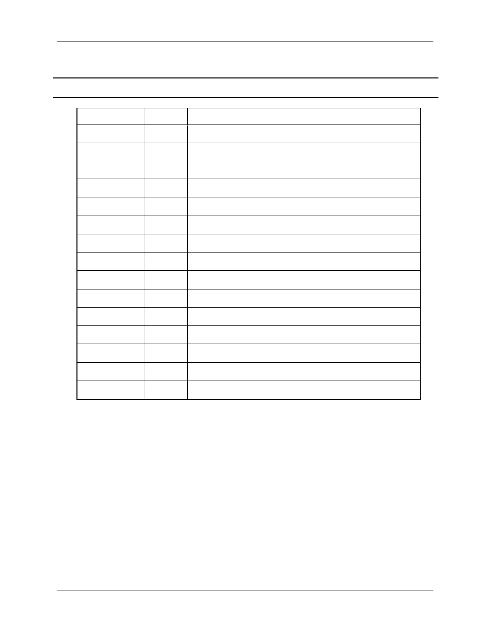
5.1. IEEE1394 Interface
This section explains the pin function of IEEE1394 interface.
Signal Name
I/O
Function
TPA0
I/O
I/O pin of TPA + (plus) signal on cable port 0
XTPA0
I/O
I/O pin of TPA - (minus) signal on cable port 0
TPB0
I/O
I/O pin of TPB + (plus) signal on cable port 0
XTPB0
I/O
I/O pin of TPB - (minus) signal on cable port 0
TPA1
I/O
I/O pin of TPA + (plus) signal on cable port 1
XTPA1
I/O
I/O pin of TPA - (minus) signal on cable port 1
TPB1
I/O
I/O pin of TPB + (plus) signal on cable port 1
XTPB1
I/O
I/O pin of TPB - (minus) signal on cable port 1
TPA2
I/O
I/O pin of TPA + (plus) signal on cable port 2
XTPA2
I/O
I/O pin of TPA - (minus) signal on cable port 2
TPB2
I/O
I/O pin of TPB + (plus) signal on cable port 2
XT PB2
I/O
I/O pin of TPB - (minus) signal on cable port 2
TPBIAS0
O
Output pin of reference voltage for common voltage on cable port 0
TPBIAS1
O
Output pin of reference voltage for common voltage on cable port 1
TPBIAS2
O
Output pin of reference voltage for common voltage on cable port 2