2 external clock (direct input), 3 internal system clock generation, 8 wake-up timer – Maxim Integrated MAXQ622 User Manual
Page 29: 2 .8 wake-up timer -25, Table 2-7 . system clock rate control settings -25, Table 2-7. system clock rate control settings
MAXQ612/MAXQ622 User’s Guide
Maxim Integrated
2-25
Crystal specifications, operating temperature, operating voltage, and parasitic capacitance must be considered when
designing the internal oscillator . The MAXQ612/MAXQ622 are designed to operate at a 12MHz maximum frequency .
To further reduce the effects of external noise, a guard ring can be placed around the oscillator circuitry .
Pins HFXIN and HFXOUT are protected by clamping devices against on-chip electrostatic discharge . These clamping
devices are diodes parasitic to the feedback resistor R
F
in the oscillator’s inverter circuit . The inverter circuit is pre-
sented as a NAND gate that can disable clock generation in stop mode .
Noise at HFXIN and HFXOUT can adversely affect on-chip clock timing . It is good design practice to place the crystal
and capacitors near the oscillator circuitry and connect to HFXIN, HFXOUT, and ground with a direct shot trace . The
typical values of external capacitors vary with the type of crystal used and should be initially selected based on the
load capacitance as suggested by the crystal manufacturer .
For cost-sensitive applications, a ceramic resonator can be used instead of a crystal . Using the ceramic resonator can
require a different circuit configuration and capacitance value .
2.7.2 External Clock (Direct Input)
The MAXQ612/MAXQ622 CPU can also obtain the system clock signal directly from an external clock source . In this
configuration, the clock generation circuitry is driven directly by an external clock .
To operate the MAXQ612/MAXQ622 from an external clock, connect the clock source to HFXIN and connect HFXOUT
to GND . The clock source should be driven through a CMOS driver . If the clock driver is a TTL gate, its output must
be connected to V
DD
through a pullup resistor to ensure a satisfactory logic level for active clock pulses . To minimize
system noise on the clock circuitry, the external clock source must meet the maximum rise and fall times and the mini-
mum high and low times specified for the clock source . The external noise can affect clock generation circuit if these
parameters do not meet the specification .
2.7.3 Internal System Clock Generation
The internal system clock is derived from the currently selected oscillator input . By default, one system clock cycle is
generated per oscillator cycle, but the number of oscillator cycles per system clock can also be increased by setting
the power-management mode enable (PMME) bit and the clock-divide control (CD[1:0]) register bits according to
Table 2-7 .
2.8 Wake-Up Timer
The MAXQ612/MAXQ622 provide a simple wake-up timer that can trigger an interrupt after a user-definable number of
internal 8kHz ring cycles . Since the wake-up timer is running off the internal ring and keeps running even during stop
mode, it can be used to wake the MAXQ612/MAXQ622 up from stop mode at periodic intervals .
To use the wake-up timer, the WUT register should be written first (before the wake-up timer is started) to define the
countdown interval . Once the time interval has been defined, the wake-up timer can be started by setting the WTE bit
to 1 . The time interval until the wake-up timer counts down to zero is defined by:
f
NANO
x WUT[15:0]
With the maximum possible time interval being:
f
NANO
x (2
16
- 1)
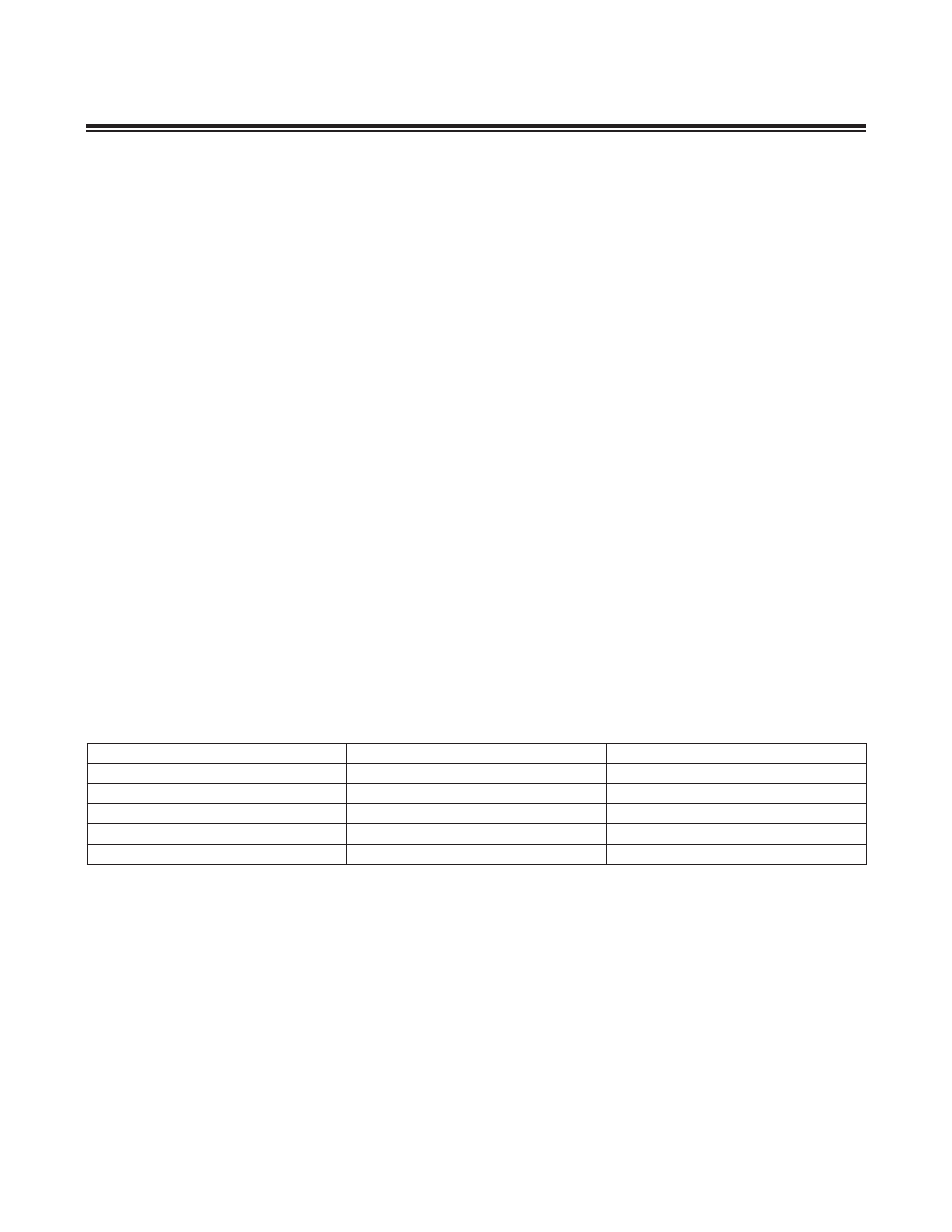
Table 2-7. System Clock Rate Control Settings
PMME
CD[1:0]
CYCLES PER CLOCK
0
00
1 (default)
0
01
2
0
10
4
0
11
8
1
xx
256