16 endpoint 1 buffer register (ep1buf), 17 endpoint 2 buffer register (ep2buf) – Maxim Integrated MAXQ622 User Manual
Page 184

MAXQ612/MAXQ622 User’s Guide
12-14
Maxim Integrated
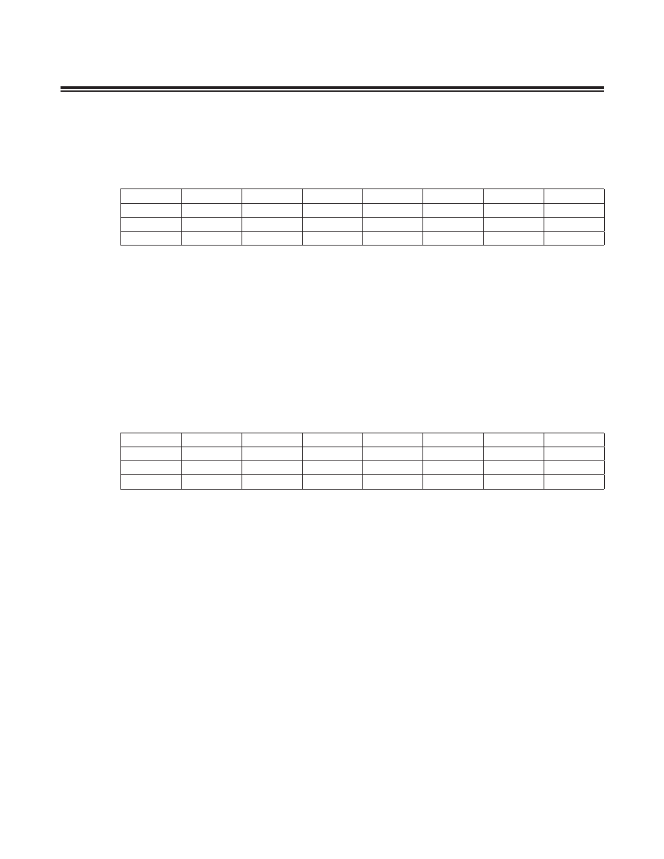
12.4.16 Endpoint 1 Buffer Register (EP1BUF)
Note: This register is indetermistic on POR and retains its value on all other forms of reset.
Note: This register is indetermistic on POR and retains its value on all other forms of reset.
Bits 7 to 0: EP1 Buffer (EP1BUF[7:0]). These data register bits are used for reading data from the double-buffered,
64-byte EP1-OUT buffer . The SIE fills the EP1-OUT buffer with bytes transmitted from the host to EP1-OUT . After suc-
cessfully receiving the OUT transfer, the SIE ACKS the transfer, updates the byte count register (EP1BC), and asserts
the OUT1DAV interrupt request .
When the CPU receives an OUT1DAV interrupt request, it reads the byte count register to determine how many bytes
are in the buffer, and then reads that number of bytes from this register .
12.4.17 Endpoint 2 Buffer Register (EP2BUF)
Bits 7 to 0: EP2 Buffer (EP2BUF[7:0]). These data register bits are used for supplying data to the double-buffered,
64-byte EP2-IN buffer . The CPU loads bytes into the EP2BUF buffer in preparation for sending to the host . The SIE
sends these bytes over USB in response to an IN request to EP2-IN .
Register Name
EP1BUF
Register Description
Endpoint 1 Buffer Register
Register Address
UADDR[4:0] = 11h
Register Name
EP2BUF
Register Description
Endpoint 2 Buffer Register
Register Address
UADDR[4:0] = 12h
Bit #
7
6
5
4
3
2
1
0
Name
EP1BUF7
EP1BUF6
EP1BUF5
EP1BUF4
EP1BUF3
EP1BUF2
EP1BUF1
EP1BUF0
Reset
s
s
s
s
s
s
s
s
Access
rw
rw
rw
rw
rw
rw
rw
rw
Bit #
7
6
5
4
3
2
1
0
Name
EP2BUF7
EP2BUF6
EP2BUF5
EP2BUF4
EP2BUF3
EP2BUF2
EP2BUF1
EP2BUF0
Reset
s
s
s
s
s
s
s
s
Access
rw
rw
rw
rw
rw
rw
rw
rw
