4 slave-receiver, 2 i2c clock generation, 11 .1 .4 slave-receiver -6 – Maxim Integrated MAXQ622 User Manual
Page 161: 11 .2 i, C clock generation -6, Figure 11-6 . i, C clock period -6, C clock generation
MAXQ612/MAXQ622 User’s Guide
11-6
Maxim Integrated
11.1.4 Slave-Receiver
The I
2
C module functions as a slave-receiver when an address match is identified (I2CAMI = 1) and the R/W bit is
0 . The I
2
C module operates in a similar fashion as the slave-transmitter mode previously described . On detecting a
START (S) condition, the I
2
C controller, if enabled, shifts in the address bits and compares it against its own address
(I2CSLA) . If the address matches, the I2CAMI flag is set to 1 and an interrupt generated if enabled . The I2CMST master
mode bit is cleared to 0 and the I2CMODE transfer mode bit is updated with the received R/W bit value of 0, indicating
that the master wants to write to the slave and the slave behaves as a receiver . On detecting this, the I
2
C controller
operates in slave-receiver mode . The I
2
C controller starts shifting into the I
2
C receive buffer when the master starts
clocking SCL . On completion of receiving a data byte, the I
2
C controller sets the receive ready interrupt flag (I2CRXI)
to 1 . This also generates an interrupt to the CPU if the receive ready interrupt is enabled (I2CRXIE = 1) . The CPU can
then read data from I2CBUF . An overrun occurs (I2CROI = 1) if the software fails to read I2CBUF when the I
2
C control-
ler receives two consecutive bytes of data . Once an overrun occurs, the I
2
C receiver always NACKs future transfers
until the I2CROI flag is cleared to 0 .
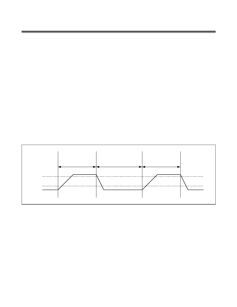
11.2 I
2
C Clock Generation
To accommodate different system needs, the I
2
C controller provides the system designer complete control over the
duty cycle of the I
2
C clock . The I
2
C peripheral is clocked by the system clock and the bit rate is defined by the I
2
C
clock control register (I2CCK) .
The high period of SCL clock is defined by the high byte of the I
2
C clock control register (I2CCKH), whereas the low
period of SCL is defined by the low byte (I2CCKL) . The minimum clock high period is three system clocks, while the
minimum low period must be at least five times the system clock period .
In master mode, the I
2
C clock characteristics are defined by the following equations:
I
2
C Low Time = System Clock Period x (I2CCKL[7:0] + 1)
I
2
C High Time = System Clock Period x (I2CCKH[7:0] + 1)
I
2
C Bit Time = (I
2
C Low Time + I
2
C High Time)
= t
SYS
x (I2CCKL[7:0] + I2CCKH[7:0] + 2)
I
2
C Bit Rate = f
SYS
/(I2CCKL[7:0] + I2CCKH[7:0] + 2)
The application can adjust SCL duty cycle accordingly while satisfying timing the requirement of the I
2
C communica-
tion channels .
During synchronization, when external masters could be driving SCL simultaneously, the actual SCL duty cycle is
affected . By monitoring the SCL state, the I
2
C controller can determine whether an external master could be holding
SCL low . In all cases, the I
2
C controller waits until the SCL has gone high before starting to count SCL high cycles .
Figure 11-6. I
2
C Clock Period
V
IH_MIN
V
IL_MAX
SCL
I2CCKH
I2CCKH
I2CCKL