Maxim Integrated MAXQ622 User Manual
Page 101
MAXQ612/MAXQ622 User’s Guide
5-28
Maxim Integrated
REGISTER
DESCRIPTION
I2CIE.11 (I2CSPIE)
I
2
C STOP Interrupt Enable. Setting this bit to 1 causes an interrupt to the CPU when a
STOP condition is detected (I2CSPI = 1) . Clearing this bit to 0 disables the STOP detection
interrupt from generating .
I2CIE.15 to I2CIE.12
Reserved. Reads return 0.
UADDR (04h, 04h)
USB Register Address Register (8-bit register) (applicable only for the MAXQ622)
Initialization:
This register is cleared to 00h on all forms of reset .
Read/Write Access:
Unrestricted read/write access except bit 6, which is read only . This register cannot be
written to when the USB controller is busy (UBUSY = 1) .
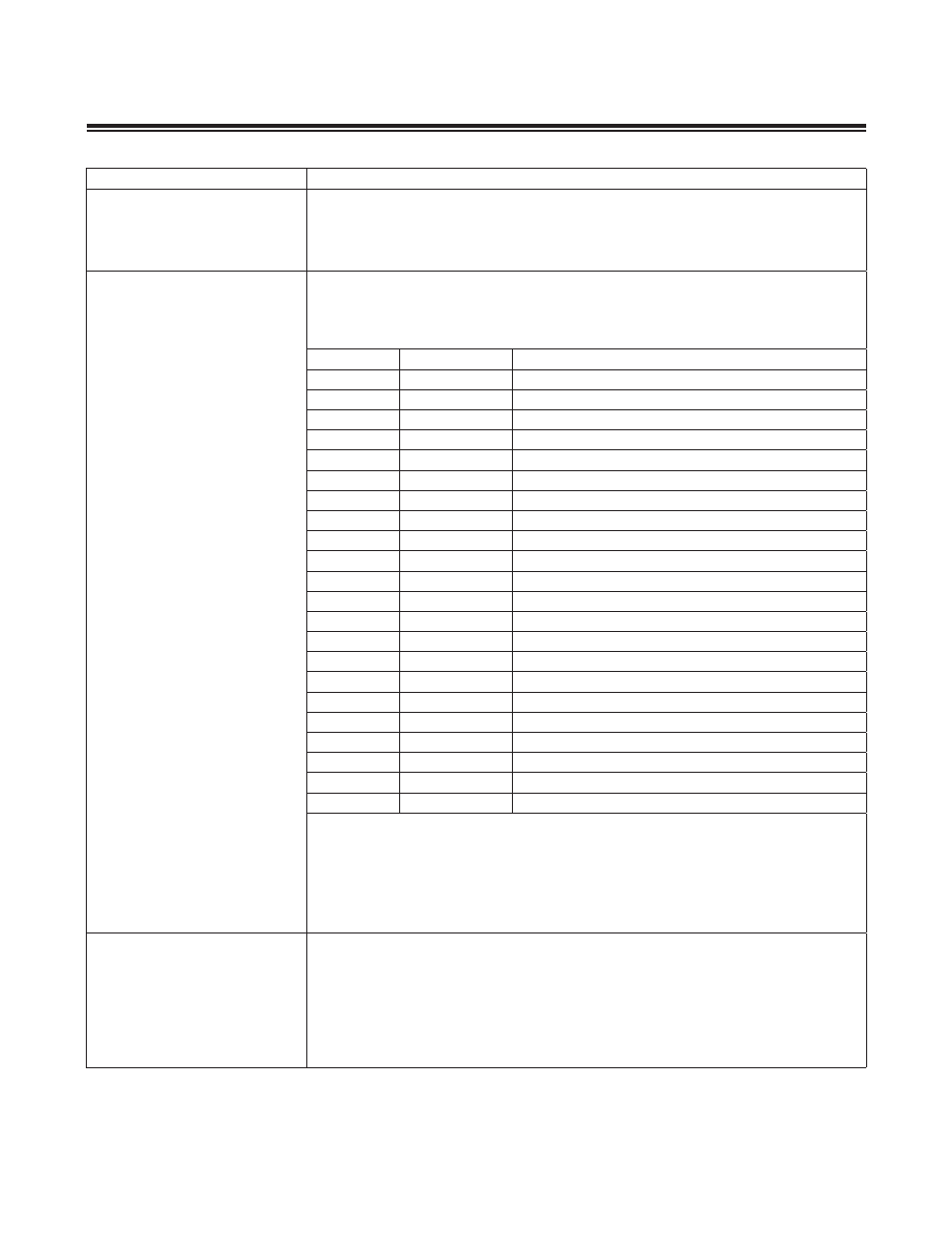
UDDR.4 to UDDR0
OFFSET
REGISTER
FUNCTION
00h
—
Idle—no operation
01h
FNADDR
Function Address Register
02h
USBCN
USB Control Register
03h
USBCFG
USB Configuration Register
04h
USBIEN
USB Interrupt Enable Register
05h
USBINT
USB Interrupt Register
06h
EPIEN
Endpoint Interrupt Enable Register
07h
EPINT
Endpoint Interrupt Register
08h
EPSTL
Endpoint Stall Register
09h
EPNAK
Endpoint NAK Register
0Ah
EPCTG
Endpoint Clear Data Toggle Register
0Bh
EP0BC
Endpoint 0 Byte Count Register
0Ch
EP1BC
Endpoint 1 Byte Count Register
0Dh
EP2BC
Endpoint 2 Byte Count Register
0Eh
EP3BC
Endpoint 3 Byte Count Register
0Fh
Reserved
No operation
10h
EP0BUF
Endpoint 0 Buffer Register
11h
EP1BUF
Endpoint 1 Buffer Register
12h
EP2BUF
Endpoint 2 Buffer Register
13h
EP3BUF
Endpoint 3 Buffer Register
14h
SUDBUF
Setup Data Buffer Register
1Fh–15h
Reserved
No operation
UADDR.5
Reserved. Reads return 0.
UADDR.6 (UBUSY)
USB Busy. This active-high busy flag is set to logic 1 to indicate the start of a USB register
read/write operation . It is held high until the end of the operation .
UADDR.7 (USBRW)
USB Register Read/Write Select. When this bit is set to 1, the CPU initiates a read
operation to the register at offset UADDR[4:0] . When cleared to 0, the CPU waits for data to
be loaded to UDATA before initiating a write operation to the register at offset UADDR[4:0] .
UDATA (05h, 04h)
USB Data Register (8-bit register) (applicable only for the MAXQ622)
Initialization:
This register is cleared to 00h on all forms of reset .
Read/Write Access:
Unrestricted read/write access except when UADDR .UBUSY = 1 . This register cannot be
written to when the USB controller is busy (UBUSY = 1) .
UDATA.7 to UDATA.0
USB Data Register Bits 7:0. These data register bits are used for supplying data for
supported USB register write operation request and for returning data for USB register read
operation .